LM25115MT/NOPB National Semiconductor, LM25115MT/NOPB Datasheet
LM25115MT/NOPB
Specifications of LM25115MT/NOPB
*LM25115MT/NOPB
LM25115MT


Related parts for LM25115MT/NOPB

LM25115MT/NOPB Summary of contents
Page 1
... Typical Application Circuit FIGURE 1. Simplified Multiple Output Power Converter Utilizing SSPR Technique © 2005 National Semiconductor Corporation Features n Self-synchronization to main channel output n Free-run mode for buck regulation of DC input ...
Page 2
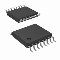
Connection Diagram Ordering Information Ordering Number Package Type LM25115MT TSSOP-16 LM25115MTX TSSOP-16 LM25115SD LM25115SDX Pin Descriptions Pin Name Description 1 CS Current Sense amplifier positive input 2 VOUT Current sense amplifier negative input 3 AGND Analog ground 4 CO Current ...
Page 3
Pin Descriptions (Continued) Pin Name Description 9 SYNC Synchronization input 10 PGND Power Ground 11 LO Low side gate driver output 12 VCC Output of bias regulator 13 HS High side MOSFET source connection 14 HO High side gate driver ...
Page 4
Block Diagram www.national.com 4 20172603 ...
Page 5
... Absolute Maximum Ratings If Military/Aerospace specified devices are required, please contact the National Semiconductor Sales Office/ Distributors for availability and specifications. VBIAS to GND VCC to GND HS to GND VOUT GND All other inputs to GND Storage Temperature Range Junction Temperature Parameter Supply Voltage, VBIAS ...
Page 6
Electrical Characteristics or HO. (Continued) Symbol Parameter CURRENT LIMIT ILIMIT Amp Transconductance Overall Transconductance Positive Current Limit Positive Current Limit Foldback VCLneg Negative Current Limit RAMP GENERATOR SYNC Input Impedance SYNC Threshold Free Run Mode Peak Threshold Current Mirror Gain ...
Page 7
Typical Performance Characteristics VCC Regulator Start-Up Characteristics, VCC vs VBIAS Current Value (CV) vs Current Limit (V Current Error Amplifier Transconductance VCC Load Regulation to Current Limit 20172604 ) Current Sense Amplifier Gain and Phase vs Frequency CL 20172606 Overall ...
Page 8
Typical Performance Characteristics Common Mode Output Voltage vs Positive Current Limit www.national.com (Continued) Common Mode Output Voltage vs Negative Current Limit (Room Temp) 20172610 8 20172611 ...
Page 9
Detailed Operating Description The LM25115 controller contains all of the features neces- sary to implement multiple output power converters utilizing the Secondary Side Post Regulation (SSPR) technique. The SSPR technique develops a highly efficient and well regu- lated auxiliary output ...
Page 10
Synchronization (SYNC) and Feed-forward (RAMP) The recommended SYNC input current range is 50µA to 150µA. The SYNC pin resistor (R SYNC set the SYNC current ( 150µA with the maximum SYNC phase signal amplitude, V PHASE(max) that I ...
Page 11
Leading Edge Pulse Width Modulation Unlike conventional voltage mode controllers, the LM25115 implements leading edge pulse width modulation. A current source equal to 3 times the I current is used to charge SYNC the capacitor connected to the RAMP pin ...
Page 12
Voltage Mode Control with Current Injection The LM25115 controller uniquely combines elements and benefits of current mode control in a voltage mode PWM controller. The current sense amplifier shown in Figure 6 monitors the inductor current as it flows through ...
Page 13
Voltage Mode Control with Current Injection Current Limiting (CS, CO and VOUT) Current limiting is implemented through the current sense amplifier as illustrated in Figure 6. The current sense ampli- fier monitors the inductor current that flows through a sense ...
Page 14
Gate Drivers Outputs (HO & LO) (Continued) mize voltage transients due to parasitic inductances and the high peak output currents of the drivers. The recommended range of the HB capacitor is 0.047µF to 0.22µF. Both drivers are controlled by the ...
Page 15
15 www.national.com ...
Page 16
Physical Dimensions www.national.com inches (millimeters) unless otherwise noted TSSOP-16 Outline Drawing NS Package Number MTC16 LLP-16 Outline Drawing NS Package Number SDA16A 16 ...
Page 17
... BANNED SUBSTANCE COMPLIANCE National Semiconductor manufactures products and uses packing materials that meet the provisions of the Customer Products Stewardship Specification (CSP-9-111C2) and the Banned Substances and Materials of Interest Specification (CSP-9-111S2) and contain no ‘‘Banned Substances’’ as defined in CSP-9-111S2. ...