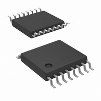
LM25115MT/NOPB National Semiconductor, LM25115MT/NOPB Datasheet - Page 13

LM25115MT/NOPB
Manufacturer Part Number
LM25115MT/NOPB
Description
IC CTRLR SSPR 42V LD REG 16TSSOP
Manufacturer
National Semiconductor
Datasheet
1.LM25115SDNOPB.pdf
(17 pages)
Specifications of LM25115MT/NOPB
Pwm Type
Voltage/Current Mode
Number Of Outputs
2
Frequency - Max
1MHz
Duty Cycle
90%
Voltage - Supply
5 V ~ 7.5 V
Buck
Yes
Boost
No
Flyback
No
Inverting
No
Doubler
No
Divider
No
Cuk
No
Isolated
No
Operating Temperature
-40°C ~ 125°C
Package / Case
16-TSSOP
Frequency-max
1MHz
Lead Free Status / RoHS Status
Lead free / RoHS Compliant
Other names
*LM25115MT
*LM25115MT/NOPB
LM25115MT
*LM25115MT/NOPB
LM25115MT
Voltage Mode Control with Current Injection
Current Limiting (CS, CO and
VOUT)
Current limiting is implemented through the current sense
amplifier as illustrated in Figure 6. The current sense ampli-
fier monitors the inductor current that flows through a sense
resistor connected between CS and VOUT. The voltage gain
of the current sense amplifier is nominally equal to 16. The
output of current sense amplifier is level shifted by 1.27V to
produce the internal CV reference signal. The CV signal
drives a current limit amplifier with nominal transconduc-
tance of 16mA/V. The current limit amplifier has an open
drain (sink only) output stage and its output pin, CO is
typically connected to the COMP pin. During normal opera-
tion, the voltage error amplifier controls the COMP pin volt-
age which adjusts the PWM duty cycle by varying the inter-
nal CRMIX level (Figure 4). However, when the current
sense input voltage V
amplifier pulls down on COMP through the CO pin. Pulling
COMP low reduces the CRMIX signal below the CV signal
level. When CRMIX does not exceed the CV signal, the
PWM comparator inhibits output pulses until the CRMIX
signal increases to a normal operating level.
A current limit fold-back feature is provided by the LM25115
to reduce the peak output current delivered to a shorted
load. When the common mode input voltage to the current
sense amplifier (CS and VOUT pins) falls below 2V, the
current limit threshold is reduced from the normal level. At
common mode voltages
nominally 45mV. When VOUT is reduced to 0V the current
limit threshold drops to 36mV to reduce stress on the induc-
tor and power MOSFETs.
CL
>
exceeds 45mV, the current limit
2V, the current limit threshold is
FIGURE 7. Voltage Sensing and Feedback
13
Negative Current Limit
When inductor current flows from the regulator output
through the low side MOSFET, the input to the current sense
comparator becomes negative. The intent of the negative
current comparator is to protect the low-side MOSFET from
excessive currents. Negative current can lead to large nega-
tive voltage spikes on the output at turn off which can dam-
age circuitry powered by the output. The negative current
comparator threshold is sufficiently negative to allow induc-
tor current to reverse at no load or light load conditions. It is
not intended to support discontinuous conduction mode with
diode emulation by the low-side MOSFET. The negative
current comparator illustrated in Figure 6 monitors the CV
signal and compares this signal to a fixed 1V threshold. This
corresponds to a negative V
VOUT of -17mV. The negative current limit comparator turns
off the low-side MOSFET for the remainder of the cycle when
the V
Gate Drivers Outputs (HO & LO)
The LM25115 provides two gate driver outputs, the floating
high-side gate driver HO and the synchronous rectifier low-
side driver LO. The low-side driver is powered directly by the
VCC regulator. The high-side gate driver is powered from a
bootstrap capacitor connected between HB and HS. An
external diode connected between VCC and HB charges the
bootstrap capacitor when the HS is low. When the high-side
MOSFET is turned on, HB rises with HS to a peak voltage
equal to VCC + V
external bootstrap diode. Both output drivers have adaptive
dead-time control to avoid shoot through currents. The adap-
tive dead-time control circuit monitors the state of each
driver to ensure that the opposing MOSFET is turned off
before the other is turned on. The HB and VCC capacitors
should be placed close to the pins of the LM25115 to mini-
CL
input falls below this threshold.
(Continued)
HS
- V
D
where V
CL
D
voltage between CS and
is the forward drop of the
20172616
www.national.com


