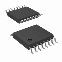
LM25115MT/NOPB National Semiconductor, LM25115MT/NOPB Datasheet - Page 12

LM25115MT/NOPB
Manufacturer Part Number
LM25115MT/NOPB
Description
IC CTRLR SSPR 42V LD REG 16TSSOP
Manufacturer
National Semiconductor
Datasheet
1.LM25115SDNOPB.pdf
(17 pages)
Specifications of LM25115MT/NOPB
Pwm Type
Voltage/Current Mode
Number Of Outputs
2
Frequency - Max
1MHz
Duty Cycle
90%
Voltage - Supply
5 V ~ 7.5 V
Buck
Yes
Boost
No
Flyback
No
Inverting
No
Doubler
No
Divider
No
Cuk
No
Isolated
No
Operating Temperature
-40°C ~ 125°C
Package / Case
16-TSSOP
Frequency-max
1MHz
Lead Free Status / RoHS Status
Lead free / RoHS Compliant
Other names
*LM25115MT
*LM25115MT/NOPB
LM25115MT
*LM25115MT/NOPB
LM25115MT
www.national.com
Voltage Mode Control with Current
Injection
The LM25115 controller uniquely combines elements and
benefits of current mode control in a voltage mode PWM
controller. The current sense amplifier shown in Figure 6
monitors the inductor current as it flows through a sense
resistor connected between CS and VOUT. The voltage gain
of the sense amplifier is nominally equal to 16. The current
sense output signal is shifted by 1.27V to produce the inter-
nal CV reference signal. The CV signal is applied to the
negative input of the PWM comparator and compared to
CRMIX as illustrated in Figure 4. Thus the PWM threshold of
the voltage mode controller (CV) varies with the instanta-
neous inductor current. Insure that the Vbias voltage is at
least 3V above the regulated output voltage (VOUT).
Injecting a signal proportional to the instantaneous inductor
current into a voltage mode controller improves the control
loop stability and bandwidth. This current injection eliminates
the lead R-C lead network in the feedback path that is
normally required with voltage mode control (see Figure 7).
Eliminating the lead network not only simplifies the compen-
sation, but also reduces sensitivity to output noise that could
pass through the lead network to the error amplifier.
FIGURE 6. Current Sensing and Limiting
12
The design of the voltage feedback path through the error
amp begins with the selection of R1 and R2 in Figure 7 to set
the regulated output voltage. The steady state output voltage
after soft-start is determined by the following equation:
The parallel impedance of the R1, R2 resistor divider should
be approximately 2k
resistance values may not be properly driven by the error
amplifier output and higher feedback resistances can intro-
duce noise sensitivity. The next step in the design process is
selection of R3, which sets the ac gain of the error amplifier.
The ac gain is given by the following equation and should be
set to a value less than 30.
The capacitor C1 is connected in series with R3 to increase
the dc gain of the voltage regulation loop and improve output
voltage accuracy. The corner frequency set by R3 x C1
should be less than 1/10th of the cross-over frequency of the
overall converter such that capacitor C1 does not add phase
lag at the crossover frequency. Capacitor C2 is added to
reduce the noise in the voltage control loop. The value of C2
should be less than 500pF and C2 may not be necessary
with very careful PC board layout.
VOUT(final) = 0.75V x (1+R1/R2)
GAIN(ac) = R3/(R1|| R2)
(between 0.5k
<
20172615
and 5k ). Lower
30


