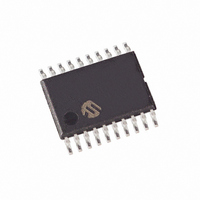
MCP1631HV-500E/ST Microchip Technology, MCP1631HV-500E/ST Datasheet - Page 6

MCP1631HV-500E/ST
Manufacturer Part Number
MCP1631HV-500E/ST
Description
IC INTEGRATED PWM HS 20TSSOP
Manufacturer
Microchip Technology
Datasheets
1.MCP1631VHVT-330EST.pdf
(34 pages)
2.MCP1631VHVT-330EST.pdf
(32 pages)
3.MCP1631HV-330EST.pdf
(54 pages)
4.MCP1631-EST.pdf
(32 pages)
Specifications of MCP1631HV-500E/ST
Package / Case
20-TSSOP
Pwm Type
Current Mode
Number Of Outputs
1
Frequency - Max
2MHz
Duty Cycle
10%
Voltage - Supply
3.5 V ~ 16 V
Buck
Yes
Boost
No
Flyback
No
Inverting
No
Doubler
No
Divider
No
Cuk
No
Isolated
Yes
Operating Temperature
-40°C ~ 125°C
Frequency-max
2MHz
Output Voltage
3.3 V to 5 V
Output Current
250 mA
Input Voltage
3 V to 5.5 V
Switching Frequency
2 MHz
Operating Temperature Range
- 40 C to + 125 C
Mounting Style
SMD/SMT
Frequency
1MHz
Digital Ic Case Style
TSSOP
No. Of Pins
20
Peak Reflow Compatible (260 C)
Yes
Rohs Compliant
Yes
Leaded Process Compatible
Yes
Lead Free Status / RoHS Status
Lead free / RoHS Compliant
For Use With
MCP1631RD-DCPC1 - REF DES BATT CHARG OR LED DRIVERMCP1631RD-MCC2 - REFERENCE DESIGN MCP1631HV
Lead Free Status / Rohs Status
Lead free / RoHS Compliant
MCP1631/HV/MCP1631V/VHV
DC CHARACTERISTICS (CONTINUED)
DS22063A-page 6
Electrical Specifications: Unless otherwise noted, V
V
External Reference Input
Reference Voltage Input
Internal Driver)
R
R
V
V
Error Amplifier (A1)
Input Offset Voltage
A1 Input Bias Current
Error Amplifier PSRR
Common Mode Input Range
Common Mode Rejection Ratio
Open-loop Voltage Gain
Low-level Output
Gain Bandwidth Product
Error Amplifier Sink Current
Error Amplifier Source Current
Current Sense (CS) Amplifier (A2)
Input Offset Voltage
CS Input Bias Current
CS Amplifier PSRR
Closed-loop Voltage Gain
Low-level Output
CS Sink Current
CS Amplifier Source Current
Voltage Sense (VS) Amplifier (A3)
Input Offset Voltage
VS Input Bias Current
Note 1:
DD
EXT
EXT
DSON
DSON
for typical values = 5.0V, T
Rise Time
Fall Time
2:
3:
4:
5:
P-channel
N-channel
Parameters
External Oscillator Input (OSC
characterization testing. Signal levels between 0.8V and 2.0V with rise and fall times measured between 10% and 90%
of maximum and minimum values. Not production tested. Additional timing specifications were fully characterized and
specified that are not production tested.
The minimum V
TCV
temperature range. V
Load regulation is measured at a constant junction temperature using low duty cycle pulse testing. Changes in output
voltage due to heating effects are determined using thermal regulation specification TCV
Dropout voltage is defined as the input to output differential at which the output voltage drops 2% below its measured
value with an applied input voltage of V
OUT
= (V
OUT-HIGH
IN
must meet two conditions: V
A
for typical values = +25°C, T
OUT-LOW
- V
R
R
I
I
OUT-LOW
GBWP
SOURCE
SOURCE
PSRR
PSRR
A2
T
T
V
DSon_N
Sym
DSon_P
A
I
I
I
I
I
V
V
V
V
V
V
BIAS
SINK
BIAS
SINK
BIAS
RISE
FALL
REF
VOL
OS
CM
OS
OS
OL
VCL
OL
IN
= lowest voltage measured over the temperature range.
) rise and fall times between 10 ns and 10 µs were determined during device
) *10
GND - 0.3
6
OUT(MAX)
/ (V
IN
Min
-0.6
-3.0
—
—
—
—
—
—
—
80
—
—
—
—
—
—
-2
-5
-5
0
4
5
5
= 3.0V to 5.5V, F
R
* ΔTemperature), V
IN
+ V
A
≥ 3.5V and V
= -40°C to +125°C for all minimum and maximums.
DROPOUT(MAX)
0.001
-19.5
0.05
85.4
0.13
17.7
-9.8
Typ
7.2
3.8
2.5
2.7
3.5
1.2
0.9
90
65
—
—
—
95
25
12
10
11
OSC
IN
GND + 65
GND + 50
≥ (V
OUT-HIGH
= 1 MHz with 10% Duty Cycle, C
AV
Max
+0.6
+3.0
V
or 3.5V, whichever is greater.
15
15
18
18
+5
—
—
—
—
—
—
—
—
—
—
1
1
1
IN
DD
OUT(MAX)
= highest voltage measured over the
Units
MHz
mV
V/V
mV
mA
mA
mV
mV
mA
mA
mV
µA
dB
dB
dB
µA
dB
µA
ns
ns
Ω
Ω
V
V
+ V
DROPOUT(MAX)
V
V
V
The reference input is capable of
rail-to-rail operation.
C
Typical for V
C
Typical for V
V
R
V
V
RL = 5 kΩ to V
V
V
V
V
lute Value
GAIN = 10
R
V
V
RL = 5 kΩ to V
© 2007 Microchip Technology Inc.
IN
IN
EAOUT
CM
IN
IN
FB
IN
FB
IN
OUT
CM
L
L
L
L
= 100 pF
= 100 pF
= 5 kΩ to V
= 5 kΩ to V
OUT
= 3.0V to 5.0V, V
= 5V, V
= 5V
= 5V, V
= 5V, V
= 3.0V to 5.0V, V
= 1.4V, V
= 1.0V, V
= 1.2V
= +0.12V
< V
.
< V
IN
Conditions
CM
REF
REF
).
IN
- 100 mV,
IN
IN
IN
COMP
COMP
- 100 mV,
= 0V to 2.5V
IN
IN
= 5V (Note 1)
= 5V (Note 1)
IN
IN
= 1.2V,
= 1.2V,
= 0.1 µF,
/2, 100 mV <
/2, 100 mV <
/2
/2
= 2.0V
= 2.0V, Abso-
CM
CM
= 1.2V
= 0.12V,


