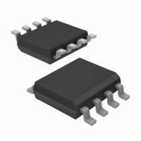
IR3637STRPBF International Rectifier, IR3637STRPBF Datasheet - Page 9

IR3637STRPBF
Manufacturer Part Number
IR3637STRPBF
Description
IC SYNC BUCK REGULATOR 8 SOIC
Manufacturer
International Rectifier
Datasheet
1.IR3637STRPBF.pdf
(21 pages)
Specifications of IR3637STRPBF
Pwm Type
Voltage Mode
Number Of Outputs
1
Frequency - Max
440kHz
Duty Cycle
85%
Voltage - Supply
4.5 V ~ 14 V
Buck
Yes
Boost
No
Flyback
No
Inverting
No
Doubler
No
Divider
No
Cuk
No
Isolated
No
Operating Temperature
0°C ~ 125°C
Package / Case
8-SOIC (3.9mm Width)
Frequency-max
440kHz
Output Current
15A
Frequency
400kHz
Supply Voltage Range
4.5V To 5.5V
Digital Ic Case Style
SOIC
No. Of Pins
8
Operating Temperature Range
0°C To +125°C
Termination Type
SMD
Rohs Compliant
Yes
Filter Terminals
SMD
Controller Type
PWM
For Use With
IRPP3637-12A - KIT REF DES 12A 1PH SYNC BUCKIRDC3637 - BOARD EVAL SYNC BUCK REGULATOR
Lead Free Status / RoHS Status
Lead free / RoHS Compliant
Other names
IR3637STRPBF
IR3637STRPBFTR
IR3637STRPBFTR
Available stocks
Company
Part Number
Manufacturer
Quantity
Price
Part Number:
IR3637STRPBF
Manufacturer:
IR
Quantity:
20 000
Note that this method requires that the output capacitor
should have enough ESR to satisfy stability requirements.
In general the output capacitor’s ESR generates a zero
typically at 5kHz to 50kHz which is essential for an ac-
ceptable phase margin.
The ESR zero of the output capacitor expressed as fol-
lows:
The transfer function (Ve / V
The (s) indicates that the transfer function varies as a
function of frequency. This configuration introduces a gain
and zero, expressed by:
The gain is determined by the voltage divider and E/A's
transconductance gain.
First select the desired zero-crossover frequency (Fo):
Use the following equation to calculate R
Rev. 1.1
06/16/05
F
H(s) = g
|H(s)| = g
F
Fo > F
R
Figure 9 - Compensation network without local
ESR
Z
4
=
=
feedback and its asymptotic gain plot.
=
V
2π×R
V
ESR
OSC
(
2π × ESR × Co
V
IN
OUT
H(s) dB
m
m
R
R
×
and F
×
1
6
5
×
4
V
Fo×F
×C
REF
Fb
Gain(dB)
R
R
6
F
1
R
×R
O
6
LC
9
R
5
+ R
≤ (1/5 ~ 1/10)× f
2
5
ESR
E/A
5
F
× R
5
Z
)
×
OUT
×
Frequency
R
Comp
4
5
) is given by:
R
+ R
R
1 + sR
C
5
4
9
Ve
sC
6
---(8)
×
9
4
C
C
S
g
POLE
1
4
m
9
:
---(10)
---(11)
---(12)
---(9)
www.irf.com
This results to R
To cancel one of the LC filter poles, place the zero be-
fore the LC filter resonant frequency pole:
Using equations (11) and (13) to calculate C
One more capacitor is sometimes added in parallel with
C
used to supress the switching noise. The additional pole
is given by:
The pole sets to one half of switching frequency which
results in the capacitor C
9
and R
Where:
V
V
Fo = Crossover Frequency
F
F
R
g
For:
V
V
Fo = 40kHz
F
F
R
R
g
F
F
For:
Lo = 1.5µH
Co = 300µF
F
R
C
Choose C
F
C
for F
m
m
ESR
LC
ESR
LC
Z
Z
Z
P
IN
OSC
IN
OSC
5
5
6
4
9
POLE
≅ 0.75 ×
and R
= Error Amplifier Transconductance
= 1.25K
= 600µmho
≅ 75%F
= 5.6kHz
= 16KΩ
= 1.77nF
=
= 1K
= Maximum Input Voltage
= 5.5V
= Resonant Frequency of the Output Filter
= 7.50kHz
4
= Zero Frequency of the Output Capacitor
= 26.5kHz
= Oscillator Ramp Voltage
= 1.25V
. This introduces one more pole which is mainly
2π × R
P
=
<<
π×R
6
9
= Resistor Dividers for Output Voltage
LC
f
2
= 1.8nF
S
4
Programming
=16.06KΩ. Choose R
2π
4
4
×f
×
1
1
S
C
C
L
-
9
1
9
O
× C
POLE:
C
+ C
1
× C
9
POLE
≅
POLE
O
IR3637SPBF
π×R
1
4
×f
4
---(13)
=16KΩ
S
9
, we get:
9


