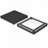
ISL6308CRZ Intersil, ISL6308CRZ Datasheet - Page 13

ISL6308CRZ
Manufacturer Part Number
ISL6308CRZ
Description
IC CTRLR PWM 3PHASE BUCK 40-QFN
Manufacturer
Intersil
Datasheet
1.ISL6308CRZ.pdf
(28 pages)
Specifications of ISL6308CRZ
Pwm Type
Voltage Mode
Number Of Outputs
1
Frequency - Max
275kHz
Duty Cycle
66.6%
Voltage - Supply
4.75 V ~ 5.25 V
Buck
Yes
Boost
No
Flyback
No
Inverting
No
Doubler
No
Divider
No
Cuk
No
Isolated
No
Operating Temperature
0°C ~ 70°C
Package / Case
40-VFQFN, 40-VFQFPN
Frequency-max
275kHz
Lead Free Status / RoHS Status
Lead free / RoHS Compliant
Available stocks
Company
Part Number
Manufacturer
Quantity
Price
Part Number:
ISL6308CRZ-T
Manufacturer:
INTERSIL
Quantity:
20 000
Load Line (Droop) Regulation
In some high current applications, a requirement on a
precisely controlled output impedance is imposed. This
dependence of output voltage on load current is often
termed “droop” or “load line” regulation.
The Droop is an optional feature in the ISL6308. It can be
enabled by connecting ICOMP pin to DROOP pin, as shown
in Figure 6. To disable it, connect the DROOP pin to IREF
pin.
As shown in Figure 6, a voltage, V
total current in all active channels, I
differential remote-sense amplifier. The resulting voltage at
the output of the remote-sense amplifier is the sum of the
output voltage and the droop voltage. As Equation 4 shows,
feeding this voltage into the compensation network causes
the regulator to adjust the output voltage so that it’s equal to
the reference voltage minus the droop voltage.
The droop voltage, V
current through the output inductors. This is accomplished
by using a continuous DCR current sensing method.
Inductor windings have a characteristic distributed
resistance or DCR (Direct Current Resistance). For
simplicity, the inductor DCR is considered as a separate
lumped quantity, as shown in Figure 7. The channel current,
I
Equation 6 shows the S-domain equivalent voltage, V
across the inductor.
The inductor DCR is important because the voltage dropped
across it is proportional to the channel current. By using a
simple R-C network and a current sense amplifier, as shown
in Figure 7, the voltage drop across all of the inductors DCRs
can be extracted. The output of the current sense amplifier,
V
currents I
If the R-C network components are selected such that the
R-C time constant matches the inductor L/DCR time
constant, then V
drops across the individual DCRs, multiplied by a gain. As
Equation 8 shows, V
total output current, I
V
V DROOP s ( )
L
V
DROOP
, flowing through the inductor, passes through the DCR.
DROOP
L
s ( )
=
, can be shown to be proportional to the channel
I
L1
L
=
⋅
, I
=
R
-------------------- - I
(
s L
COMP
L2
------------------------------------------------------------------------- -
(
R
⋅
s R
, and I
⋅
S
DROOP
+
COMP
DCR
⋅
⎛
⎝
DROOP
OUT
DROOP
-------------
DCR
OUT
s L
L3
⋅
)
⋅
, shown in Equation 7.
is equal to the sum of the voltage
C
.
+
⋅
COMP
DCR
1
⎞
⎠
, is created by sensing the
is therefore proportional to the
13
+
DROOP
1
)
OUT
⋅
R
-----------------------
COMP
R
, feeds into the
S
, proportional to the
⋅
(
I L1
+
I L2
L
+
(EQ. 6)
(EQ. 7)
(EQ. 8)
,
I L3
) DCR
⋅
ISL6308
By simply adjusting the value of R
to any level, giving the converter the right amount of droop at
all load currents. It may also be necessary to compensate for
any changes in DCR due to temperature. These changes
cause the load line to be skewed, and cause the R-C time
constant to not match the L/DCR time constant. If this
becomes a problem a simple negative temperature
coefficient resistor network can be used in the place of
R
temperature.
Output Voltage Offset Programming
The ISL6308 allows the designer to accurately adjust the
offset voltage by connecting a resistor, R
pin to VCC or GND. When R
and VCC, the voltage across it is regulated to 1.5V. This
causes a proportional current (I
and out of the FB pin. If R
voltage across it is regulated to 0.5V, and I
FB pin and out of the OFS pin. The offset current flowing
through the resistor between VDIFF and FB will generate
the desired offset voltage which is equal to the product
(I
OFS
COMP
V
ISL6308
DROOP
x R
+
-
to compensate for the rise in DCR due to
FIGURE 7. DCR SENSING CONFIGURATION
1
PHASE1
PHASE2
). These functions are shown in Figures 8 and 9.
DROOP
IREF
ICOMP
ISUM
C
SUM
(Optional)
OFS
C
COMP
OFS
R
S
is connected to ground, the
OFS
is connected between OFS
R
R
S
S
COMP
, the load line can be set
) to flow into the OFS pin
I
I
L2
L1
INDUCTOR
INDUCTOR
L1
L2
OFS
V
OFS
L
(s)
, from the OFS
DCR
DCR
-
September 30, 2008
flows into the
FN9208.4
C
I
OUT
V
OUT
OUT


