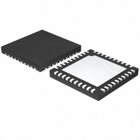
ISL6308CRZ Intersil, ISL6308CRZ Datasheet - Page 26

ISL6308CRZ
Manufacturer Part Number
ISL6308CRZ
Description
IC CTRLR PWM 3PHASE BUCK 40-QFN
Manufacturer
Intersil
Datasheet
1.ISL6308CRZ.pdf
(28 pages)
Specifications of ISL6308CRZ
Pwm Type
Voltage Mode
Number Of Outputs
1
Frequency - Max
275kHz
Duty Cycle
66.6%
Voltage - Supply
4.75 V ~ 5.25 V
Buck
Yes
Boost
No
Flyback
No
Inverting
No
Doubler
No
Divider
No
Cuk
No
Isolated
No
Operating Temperature
0°C ~ 70°C
Package / Case
40-VFQFN, 40-VFQFPN
Frequency-max
275kHz
Lead Free Status / RoHS Status
Lead free / RoHS Compliant
Available stocks
Company
Part Number
Manufacturer
Quantity
Price
Part Number:
ISL6308CRZ-T
Manufacturer:
INTERSIL
Quantity:
20 000
and lead to device overvoltage stress. Careful component
layout and printed circuit design minimizes the voltage
spikes in the converter. Consider, as an example, the turnoff
transition of the upper PWM MOSFET. Prior to turnoff, the
upper MOSFET was carrying channel current. During the
turnoff, current stops flowing in the upper MOSFET and is
picked up by the lower MOSFET. Any inductance in the
switched current path generates a large voltage spike during
the switching interval. Careful component selection, tight
layout of the critical components, and short, wide circuit
traces minimize the magnitude of voltage spikes.
There are two sets of critical components in a DC/DC
converter using a ISL6308 controller. The power
components are the most critical because they switch large
amounts of energy. Next are small signal components that
connect to sensitive nodes or supply critical bypassing
current and signal coupling.
It is important to have a symmetrical layout, preferably with
the controller equidistantly located from the three power
trains it controls. Equally important are the gate drive lines
(UGATE, LGATE, PHASE): since they drive the power train
MOSFETs using short, high current pulses, it is important to
size them as large and as short as possible to reduce their
overall impedance and inductance. Extra care should be
given to the LGATE traces in particular since keeping the
impedance and inductance of these traces helps to
significantly reduce the possibility of shoot-through.
Equidistant placement of the controller to the three power
trains also helps to keep these traces equally short (equal
impedances, resulting in similar driving of both sets of
MOSFETs).
The power components should be placed first. Locate the
input capacitors close to the power switches. Minimize the
length of the connections between the input capacitors, C
and the power switches. Locate the output inductors and
Intersil products are sold by description only. Intersil Corporation reserves the right to make changes in circuit design, software and/or specifications at any time without
notice. Accordingly, the reader is cautioned to verify that data sheets are current before placing orders. Information furnished by Intersil is believed to be accurate and
reliable. However, no responsibility is assumed by Intersil or its subsidiaries for its use; nor for any infringements of patents or other rights of third parties which may result
from its use. No license is granted by implication or otherwise under any patent or patent rights of Intersil or its subsidiaries.
All Intersil U.S. products are manufactured, assembled and tested utilizing ISO9000 quality systems.
Intersil Corporation’s quality certifications can be viewed at www.intersil.com/design/quality
For information regarding Intersil Corporation and its products, see www.intersil.com
26
IN
,
ISL6308
output capacitors between the MOSFETs and the load.
Locate the high-frequency decoupling capacitors (ceramic)
as close as practicable to the decoupling target, making use
of the shortest connection paths to any internal planes, such
as vias to GND immediately next, or even onto the capacitor
solder pad.
The critical small components include the bypass capacitors
for VCC and PVCC. Locate the bypass capacitors, CBP,
close to the device. It is especially important to locate the
components associated with the feedback circuit close to
their respective controller pins, since they belong to a high
impedance circuit loop, sensitive to EMI pick-up. It is also
important to place current sense components close to their
respective pins on the ISL6308, including the RISEN
resistors, RS, RCOMP, CCOMP. For proper current sharing
route three separate symmetrical as possible traces from the
corresponding phase node for each RISEN.
A multi-layer printed circuit board is recommended. Figure 27
shows the connections of the critical components for the
converter. Note that capacitors C
each represent numerous physical capacitors. Dedicate one
solid layer, usually the one underneath the component side
of the board, for a ground plane and make all critical
component ground connections with vias to this layer.
Dedicate another solid layer as a power plane and break this
plane into smaller islands of common voltage levels. Keep
the metal runs from the PHASE terminal to inductor L
short. The power plane should support the input power and
output power nodes. Use copper filled polygons on the top
and bottom circuit layers for the phase nodes. Use the
remaining printed circuit layers for small signal wiring. The
wiring traces from the IC to the MOSFETs’ gates and
sources should be sized to carry at least one ampere of
current (0.02” to 0.05”).
xxIN
and C
xxOUT
September 30, 2008
could
OUT
FN9208.4


