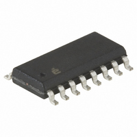
ISL6740IBZ Intersil, ISL6740IBZ Datasheet - Page 22

ISL6740IBZ
Manufacturer Part Number
ISL6740IBZ
Description
IC CTRLR PWM DBL-ENDED 16-SOIC
Manufacturer
Intersil
Datasheet
1.ISL6741IVZ.pdf
(29 pages)
Specifications of ISL6740IBZ
Pwm Type
Voltage Mode
Number Of Outputs
2
Frequency - Max
2MHz
Duty Cycle
100%
Voltage - Supply
9 V ~ 16 V
Buck
No
Boost
No
Flyback
No
Inverting
No
Doubler
No
Divider
No
Cuk
No
Isolated
No
Operating Temperature
-40°C ~ 105°C
Package / Case
16-SOIC (3.9mm Width)
Frequency-max
2MHz
Lead Free Status / RoHS Status
Lead free / RoHS Compliant
Available stocks
Company
Part Number
Manufacturer
Quantity
Price
Company:
Part Number:
ISL6740IBZ
Manufacturer:
Intersil
Quantity:
122
Adding Line Only Regulation - Feed Forward
Output voltage variation caused by changes in the supply
voltage may be virtually removed through a technique known
as feed forward compensation. Using feed forward, the duty
cycle is directly controlled based on changes in the input
voltage only. No closed loop feedback system is required.
Voltage feed forward may be implemented as shown in
Figure 18..
The circuit provides feed forward compensation for a 2:1
input voltage range. Resistors R
voltage divider to generate a 1V signal at the input voltage
that corresponds to maximum duty cycle (V
Resistors R
VREF to create reference voltages for the amplifiers. The
first stage uses U
a unity gain inverting amplifier. Its output varies inversely
with input voltage and ranges from 1V to 2V. The bandwidth
of the circuit may be controlled by varying the value of C
The gain of the first amplifier stage is:
V
where:
V
V
The second stage uses U
to form a summing amplifier which offsets the first stage
output by 0.8V (the value of C
applied to the V
amplitude of the oscillator sawtooth so that the duty cycle
varies linearly from 100% to 50% of maximum with a 2:1
input voltage variation.
A
A
D
= Output voltage of U
=
= The input divider voltage
69.8k
R100
R101
VREF
2k
–
FIGURE 18. VOLTAGE FEED FORWARD CIRCUIT
V
D
+VIN
+
3.48k
R109
109
3.00
R102
100k
, R
ERROR
100A
110
1.5V
V
49.9k
R103
, and R
+
-
C100
R104
100k
, R
1nF
input now matches the offset and
U100A
100A
102
R110
100B
698
, R
111
22
T
R105
100k
, R
103
valley voltage). The signal
0.8V
100
form a voltage divider from
105
R108
100k
, R
and R
, R
104
R111
-
+
R106
R107
100k
100K
806
106
U100B
, and C
101
, R
IN
107
minimum).
set the input
100
, and R
to VERROR
ISL6740, 1SL6741
to form
(EQ. 25)
100
108
.
Other duty ranges are possible, but are still limited to a 2:1
ratio. The voltage applied to V
peak-to-peak voltage on C
Since the peak-to-peak C
voltage at the output of U100A must be divided by 2.0V to
obtain the desired duty cycle. For example, if an 80% duty
cycle was required at the minimum operating voltage, the
output of U100A must be 1.60V (80% of 2.00V). From
(Equation 25), the divider voltage must be set to 1.4V for the
input voltage that corresponds to the 80% duty cycle.
It should be noted that the synchronous rectifiers (SRs),
being driven from the transformer secondary, are only gated
on during the ON time of the primary FETs. Conduction
continues through the body diodes during the OFF time
when operating in continuous inductor current mode. This
mode of operation usually results in significant conduction
and switching losses in the SR FETs. These losses may be
reduced considerably by either adding schottky diodes in
parallel to the SR FETs or by driving the SR FETs directly
with a control signal.
Adding Regulation - Closed Loop Feedback
The second Typical Application schematic adds closed loop
feedback with isolation. The ISL6740EVAL2Z demonstration
platform implements this design and is available for
evaluation. The input voltage range was increased to 36V to
75V, which necessitates a few modifications to the open loop
design. The output inductor value was increased to 4.0μH,
schottky rectifier CR4 was added to minimize SR FET body
diode conduction, the turns ratio of the main transformer was
changed to 4:3, and the synchronous rectifier gate drives
were modified. The design process is essentially the same
as it was for the unregulated version, so only the feedback
control loop design will be discussed.
The major components of the feedback control loop are a
programmable shunt regulator and an opto-coupler. The
opto-coupler is used to transfer the error signal across the
isolation barrier. The opto-coupler offers a convenient means
to cross the isolation barrier, but it adds complexity to the
feedback control loop. It adds a pole at about 10kHz and a
significant amount of gain variation due the current transfer
ratio (CTR). The CTR of the opto-coupler varies with initial
tolerance, temperature, forward current, and age.
T
T
, and offset by the valley voltage.
voltage is 2.00V nominal, the
ERROR
must be scaled to the
July 13, 2007
FN9111.4


