ISL6742AAZA-T Intersil, ISL6742AAZA-T Datasheet - Page 15

ISL6742AAZA-T
Manufacturer Part Number
ISL6742AAZA-T
Description
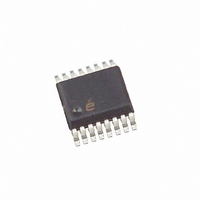
IC CTRLR PWM DBL ENDED 16-QSOP
Manufacturer
Intersil
Datasheet
1.ISL6742AAZA.pdf
(18 pages)
Specifications of ISL6742AAZA-T
Pwm Type
Voltage/Current Mode
Number Of Outputs
4
Frequency - Max
2MHz
Duty Cycle
100%
Voltage - Supply
9 V ~ 16 V
Buck
No
Boost
No
Flyback
No
Inverting
No
Doubler
No
Divider
No
Cuk
No
Isolated
No
Operating Temperature
-40°C ~ 105°C
Package / Case
16-QSOP
Frequency-max
2MHz
Lead Free Status / RoHS Status
Lead free / RoHS Compliant
Other names
ISL6742AAZA-TTR
Available stocks
Company
Part Number
Manufacturer
Quantity
Price
Company:
Part Number:
ISL6742AAZA-T
Manufacturer:
Intersil
Quantity:
2 000
Part Number:
ISL6742AAZA-T
Manufacturer:
INTERSIL
Quantity:
20 000
If ΔV
compensation is needed and R
If ΔV
value of R
by the external ramp must be reduced by ΔV
Adding slope compensation is accomplished in the ISL6742
using an external buffer and the CT signal. A typical
application sums the buffered CT signal with the current
sense feedback and applies the result to the CS pin as
shown in Figure 14.
Assuming the designer has selected values for the RC filter
(R6 and C4) placed on the CS pin, the value of R9 required
to add the appropriate external ramp can be found by
superposition.
Rearranging to solve for R9 yields:
The value of R
rescaled so that the current sense signal presented at the
CS pin is that predicted by Equation 17. The divider created
by R6 and R9 makes this necessary.
R
V
R9
R′
e
CS
CS
–
=
CS
CS
ΔV
=
=
(
------------------------------------------------------------ -
2D V
CS
--------------------------------------------------------------------------------------------------------------------------------- -
N
------- -
N
is greater than or equal to Ve, then no additional slope
is less than V
FIGURE 14. ADDING SLOPE COMPENSATION
R6
--------------------- - R
S
P
CS
–
R9
⋅
=
V
+
⎛
⎜
⎝
I
, but the amount of slope compensation added
e
R9
e
--------------------- -
R6
O
2D R6
–
+
CS
+
ΔV
ΔV
⋅
+
⋅
Dt
-------------- -
R
2L
R9
determined in Equation 19 must be
CS
CS
CS
SW
CS
O
e
) R6
, then Equation 19 is still valid for the
⋅
⋅
⎛
⎜
⎝
V
IN
V
R9
C4
R6
N
⋅
15
CT
N
------- -
N
CS
S
P
Ω
–
becomes Equation 22:
V
O
⎞
⎟
⎠
⎞
⎟
⎠
+
V
-----------------------------
IN
CT
1
2
3
4
5
6
7
8
CS
L
⋅
VREF
CT
CS
Dt
m
.
SW
ISL6742
(EQ. 22)
(EQ. 23)
(EQ. 24)
(EQ. 25)
ISL6742
16
15
14
13
12
11
10
9
Example:
V
V
L
N
Lm = 2mH
I
Oscillator Frequency, F
Duty Cycle, D = 85.7%
N
R6 = 499Ω
Solve for the current sense resistor, R
R
Determine the amount of voltage, V
the current feedback signal using Equation 16.
V
Next, determine the effect of the magnetizing current from
Equation 21.
ΔV
Using Equation 24, solve for the summing resistor, R9, from
CT to CS.
R9 = 13.2kΩ
Determine the new value of R
R’
Additional slope compensation may be considered for
design margin. This discussion determines the minimum
external ramp that is required. The buffer transistor used to
create the external ramp from CT should have a sufficiently
high gain (>200) so as to minimize the required base
current. Whatever base current is required reduces the
charging current into CT and will reduce the oscillator
frequency.
Parallel Operation
Parallel operation of converters using the ISL6742 may be
accomplished using the average current signal, IOUT. IOUT
provides a very accurate representation of the output current
and may be used for active current sharing with many
sharing techniques commonly used including master-slave
and average current sharing methods.
Since IOUT represents the average inductor current (CCM
operation), sharing errors introduced by techniques using
peak inductor current are reduced. In particular, the current
sharing error introduced by mismatched switching
frequencies is eliminated.
O
O
IN
O
e
P
CT
CS
CS
= 55A
/N
CS
= 153mV
= 2.0µH
= 12V
= 280V
= 50
= 15.1Ω.
S
= 15.7Ω
= 91mV
= 20
SW
= 400kHz
CS
, R’
e
CS
, that must be added to
CS
, using Equation 25.
, using Equation 19.
October 31, 2008
FN9183.2


