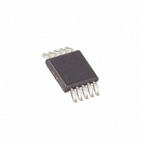
MAX668EUB+T Maxim Integrated Products, MAX668EUB+T Datasheet - Page 12

MAX668EUB+T
Manufacturer Part Number
MAX668EUB+T
Description
IC PWM BST FLYBCK ISO CM 10UMAX
Manufacturer
Maxim Integrated Products
Datasheet
1.MAX669EUB.pdf
(18 pages)
Specifications of MAX668EUB+T
Pwm Type
Current Mode
Number Of Outputs
1
Frequency - Max
575kHz
Duty Cycle
94%
Voltage - Supply
3 V ~ 28 V
Buck
No
Boost
Yes
Flyback
Yes
Inverting
No
Doubler
No
Divider
No
Cuk
No
Isolated
Yes
Operating Temperature
-40°C ~ 85°C
Package / Case
10-MSOP, Micro10™, 10-uMAX, 10-uSOP
Frequency-max
575kHz
Lead Free Status / RoHS Status
Lead free / RoHS Compliant
1.8V to 28V Input, PWM Step-Up
Controllers in µMAX
Table 2. Bootstrapped and Non-Bootstrapped Configurations
* For standard step-up DC-DC circuits (as in Figures 2, 3, 4, and 5), regulation cannot be maintained if V
In addition to the configurations shown in Table 2, the
following guidelines may help when selecting a config-
uration:
1) If V
2) If V
12
High-Voltage,
Bootstrapped
Low-Voltage,
Bootstrapped
High-Voltage,
Non-Bootstrapped
Low-Voltage,
Non-Bootstrapped
Extra IC supply,
Non-Bootstrapped
CONFIGURATION
and transformer-based circuits do not have this limitation.
strapped to V
V
V
the LDO regulator.
from V
This can save quiescent power consumption, espe-
cially when V
5.5V, LDO may be shorted to V
nate the dropout voltage of the LDO regulator.
______________________________________________________________________________________
OUT
CC
IN
IN
and V
never exceeds 5.5V, LDO may be shorted to
IN
is ever below 2.7V, V
is greater than 3V, V
, rather than from V
OUT
OUT
OUT
FIGURE
to eliminate the dropout voltage of
Figure
Figure
Figure
Figure
None
and the MAX669 must be used. If
2
3
4
5
is large. If V
MAX669
MAX669
MAX668
MAX668
MAX668
WITH:
OUT
USE
CC
CC
CC
(non-bootstrapped).
IN
can be powered
and V
must be boot-
never exceeds
RANGE* (V)
VOLTAGE
Restricted
1.8 to 5.5
2.7 to 5.5
1.8 to 28
3 to 28
INPUT
Not
IN
to elimi-
RANGE (V)
VOLTAGE
2.7 to 5.5
OUTPUT
3V to 28
V
V
V
IN
IN
IN
to ∞
to ∞
to ∞
3) If V
4) If V
3-cell NiMH battery range), bootstrapping V
V
efficiency by increasing gate drive (and reducing
FET resistance) at the expense of quiescent power
consumption.
V
increase gate drive from EXT but does increase
quiescent power dissipation.
OUT
IN
IN
IN
, since bootstrapping from V
Connect V
FET gate drive for low-voltage (Input <3V) to high-
voltage (output >5.5V) boost circuits. V
exceed 28V.
Connect V
mum possible external FET gate drive for low-volt-
age designs, but limits V
Connect V
put range, but external FET gate drive is reduced for
V
Connect V
amplitude = V
high-voltage (output >5.5V) boost circuits. IC oper-
ating power is less than in Figure 4, since IC current
does not pass through the LDO regulator.
Connect V
(V
amplitude = V
output voltage range (V
except that V
IN
, although not required, may increase overall
BIAS
always exceeds 4.5V, V
is in the 3V to 4.5V range (i.e., 1-cell Li+ or
below 5V.
) that powers only the IC. FET gate-drive
CC
OUT
IN
IN
CC
OUT
to V
to V
IN
BIAS
to V
and LDO to a separate supply
to V
for logic-supply (input 3V to 5.5V) to
must exceed V
CC
CC
. Input power source (V
OUT
COMMENTS
CC
. Provides widest input and out-
and LDO. FET gate-drive
. Provides maximum external
and LDO. Provides maxi-
OUT
OUT
IN
) are not restricted,
exceeds V
to 5.5V or less.
CC
IN
.
should be tied to
OUT
OUT
OUT
IN)
. SEPIC
does not
cannot
and
CC
from


