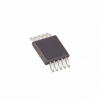
MAX668EUB+T Maxim Integrated Products, MAX668EUB+T Datasheet - Page 14

MAX668EUB+T
Manufacturer Part Number
MAX668EUB+T
Description
IC PWM BST FLYBCK ISO CM 10UMAX
Manufacturer
Maxim Integrated Products
Datasheet
1.MAX669EUB.pdf
(18 pages)
Specifications of MAX668EUB+T
Pwm Type
Current Mode
Number Of Outputs
1
Frequency - Max
575kHz
Duty Cycle
94%
Voltage - Supply
3 V ~ 28 V
Buck
No
Boost
Yes
Flyback
Yes
Inverting
No
Doubler
No
Divider
No
Cuk
No
Isolated
Yes
Operating Temperature
-40°C ~ 85°C
Package / Case
10-MSOP, Micro10™, 10-uMAX, 10-uSOP
Frequency-max
575kHz
Lead Free Status / RoHS Status
Lead free / RoHS Compliant
given output ripple. An inductance value larger than
L
must be increased by the same proportion that L has to
L
information on determining output filter values.
Due the MAX668/MAX669’s high switching frequencies,
inductors with a ferrite core or equivalent are recom-
mended. Powdered iron cores are not recommended
due to their high losses at frequencies over 50kHz.
The peak inductor current required for a particular out-
put is:
where I
the inductor peak-to-peak ripple current. The I
I
where V
Schottky rectifier diode (D1), and V
across the external FET, when on.
where L is the inductor value. The saturation rating of
the selected inductor should meet or exceed the calcu-
lated value for I
operated up to 20% over their saturation rating without
difficulty. In addition to the saturation criteria, the induc-
tor should have as low a series resistance as possible.
For continuous inductor current, the power loss in the
inductor resistance, P
where R
Once the peak inductor current is selected, the current-
sense resistor (R
For high peak inductor currents (>1A), Kelvin sensing
connections should be used to connect CS+ and
PGND to R
at the ground side of R
The MAX668/MAX669 drive a wide variety of N-channel
power MOSFETs (NFETs). Since LDO limits the EXT
output gate drive to no more than 5V, a logic-level
NFET is required. Best performance, especially at low
input voltages (below 5V), is achieved with low-thresh-
1.8V to 28V Input, PWM Step-Up
Controllers in µMAX
14
LPP
IDEAL
IDEAL
terms are determined as follows:
______________________________________________________________________________________
I
LPP
. See the Capacitor Selection section for more
LDC
may also be used, but output-filter capacitance
L
D
is the inductor series resistance.
Determining Peak Inductor Current
CS
=
is the forward voltage drop across the
is the average DC input current and I
P
LR
. PGND and GND should be tied together
I
(V
LDC
I
LPEAK
LPEAK
IN
CS
R
(I
CS
) is determined by:
L x f
OUT
– V
=
LR
, although most coil types can be
= 85mV / I
= I
Power MOSFET Selection
CS
I
SW
OUT
OSC
, is approximated by:
x V
LDC
.
(V
) (V
OUT
IN
(V
OUT
+ (I
(V
OUT
– V
OUT
/ V
LPEAK
LPP
SW
+ V
IN
+ V
+ V )
)
/ 2)
2
)
D
D
x R
SW
D
)
– V )
L
is the drop
IN
LDC
LPP
and
is
old NFETs that specify on-resistance with a gate-
source voltage (V
NFET, key parameters can include:
1) Total gate charge (Q
2) Reverse transfer capacitance or charge (C
3) On-resistance (R
4) Maximum drain-to-source voltage (V
5) Minimum threshold voltage (V
At high switching rates, dynamic characteristics (para-
meters 1 and 2 above) that predict switching losses
may have more impact on efficiency than R
which predicts DC losses. Q
associated with charging the gate. In addition, this
parameter helps predict the current needed to drive the
gate at the selected operating frequency. The continu-
ous LDO current for the FET gate is:
For example, the MMFT3055L has a typical Q
(at V
3.5mA. Use the FET manufacturer’s typical value for Q
in the above equation, since a maximum value (if sup-
plied) is usually too conservative to be of use in esti-
mating I
The MAX668/MAX669’s high switching frequency
demands a high-speed rectifier. Schottky diodes are
recommended for most applications because of their
fast recovery time and low forward voltage. Ensure that
the diode’s average current rating is adequate using
the diode manufacturer’s data, or approximate it with
the following formula:
Also, the diode reverse breakdown voltage must
exceed V
Schottky diodes may not be practical because of this
voltage requirement. In these cases, use a high-speed
silicon rectifier with adequate reverse voltage.
The minimum output filter capacitance that ensures sta-
bility is:
where V
Typically C
GS
C
= 5V); therefore, the I
GATE
OUT(MIN)
IN(MIN)
OUT
OUT(MIN)
I
.
DIODE
. For high output voltages (50V or above),
is the minimum expected input voltage.
GS
I
GATE
) of 2.7V or less. When selecting an
, though sufficient for stability, will
DS(ON)
I
(2 R
OUT
g
= Q
(7.5V x L / L
)
CS
)
g
g
I
GATE
LPEAK
Capacitor Selection
includes all capacitances
x V
x f
Output Filter Capacitor
OSC
IN(MIN)
TH(MIN)
Diode Selection
current at 500kHz is
3
- I
IDEAL
OUT
DS(MAX)
)
x f
OSC
)
RSS
g
)
)
DS(ON),
of 7nC
)
g


