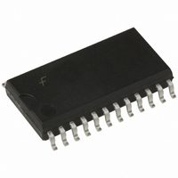
FAN5059MX Fairchild Semiconductor, FAN5059MX Datasheet - Page 12

FAN5059MX
Manufacturer Part Number
FAN5059MX
Description
IC CTRLR DC/DC PROG SYNC 24SOIC
Manufacturer
Fairchild Semiconductor
Datasheet
1.FAN5059MX.pdf
(18 pages)
Specifications of FAN5059MX
Applications
Controller, VRM8.5
Voltage - Input
5V
Number Of Outputs
1
Voltage - Output
1.3 ~ 3.5 V
Operating Temperature
0°C ~ 70°C
Mounting Type
Surface Mount
Package / Case
24-SOIC (7.5mm Width)
Output Current
18 A
Input Voltage
5 V
Mounting Style
SMD/SMT
Lead Free Status / RoHS Status
Lead free / RoHS Compliant
Other names
FAN5059MXTR
FAN5059MX_NL
FAN5059MX_NLTR
FAN5059MX_NLTR
FAN5059MX_NL
FAN5059MX_NLTR
FAN5059MX_NLTR
Available stocks
Company
Part Number
Manufacturer
Quantity
Price
Company:
Part Number:
FAN5059MX
Manufacturer:
MITEL
Quantity:
500
Part Number:
FAN5059MX
Manufacturer:
FAIRCHILD/ن»™ç«¥
Quantity:
20 000
FAN5059
Test Parameters
Application Information
The FAN5059 Controller
The FAN5059 is a programmable synchronous DC-DC con-
troller IC. When designed around the appropriate external
components, the FAN5059 can be configured to deliver more
than 16A of output current, as appropriate for the Katmai and
Coppermine and other processors. The FAN5059 functions
as a fixed frequency PWM step down regulator.
Main Control Loop
Refer to the FAN5059 Block Diagram on page 1. The
FAN5059 implements “summing mode control”, which is dif-
ferent from both classical voltage-mode and current-mode
control. It provides superior performance to either by allow-
ing a large converter bandwidth over a wide range of output
loads.
The control loop of the regulator contains two main sections:
the analog control block and the digital control block. The
analog section consists of signal conditioning amplifiers feeding
into a comparator which provides the input to the digital control
block. The signal conditioning section accepts input from the
DROOP (current feedback) and VFB (voltage feedback) pins
and sets up two controlling signal paths. The first, the voltage
control path, amplifies the difference between the VFB signal
and the reference voltage from the DAC and presents the
output to one of the summing amplifier inputs. The second,
current control path, takes the difference between the DROOP
and SW pins when the high-side MOSFET is on, reproducing
the voltage across the MOSFET and thus the input current; it
presents the resulting signal to another input of the summing
amplifier. These two signals are then summed together. This
output is then presented to a comparator looking at the oscillator
ramp, which provides the main PWM control signal to the
digital control block.
The digital control block takes the analog comparator input
and the main clock signal from the oscillator to provide the
appropriate pulses to the HIDRV and LODRV output pins.
These two outputs control the external power MOSFETs.
There is an additional comparator in the analog control section
whose function is to set the point at which the FAN5059 cur-
rent limit comparator disables the output drive signals to the
external power MOSFETs.
12
t
DT
2V
Figure 3. Ouput Drive Timing Diagram
t
2V
R
5V
5V
2V
t
F
2V
t
DT
LODRV
HIDRV
to SW
High Current Output Drivers
The FAN5059 contains two identical high current output driv-
ers that utilize high speed bipolar transistors in a push-pull
configuration. The drivers’ power and ground are separated
from the chip’s power and ground for switching noise immu-
nity. The power supply pin, VCCP, is supplied from an exter-
nal 12V source through a series 33 resistor. The resulting
voltage is sufficient to provide the gate to source drive to the
external MOSFETs required in order to achieve a low R
Internal Voltage Reference
The reference included in the FAN5059 is a precision band-
gap voltage reference. Its internal resistors are precisely
trimmed to provide a near zero temperature coefficient (TC).
Based on the reference is the output from an integrated 5-bit
DAC. The DAC monitors the 5 voltage identification pins,
VID0-4. When the VID4 pin is at logic HIGH, the DAC
scales the reference voltage from 2.0V to 3.5V in 100mV
increments. When VID4 is pulled LOW, the DAC scales the
reference from 1.30V to 2.05V in 50mV increments. All VID
codes are available, including those below 1.80V.
Power Good (PWRGD)
The FAN5059 Power Good function is designed in accor-
dance with the Pentium II and III DC-DC converter specifi-
cations and provides a continuous voltage monitor on the
VFB pin. The circuit compares the VFB signal to the VREF
voltage and outputs an active-low interrupt signal to the CPU
should the power supply voltage deviate more than ±16% of
its nominal setpoint. Power Good outputs an open collector
high when the output voltage is within ±12% of its nominal
setpoint. The Power Good flag provides no other control
function to the FAN5059.
Output Enable/Soft Start (ENABLE/SS)
The FAN5059 will accept an open collector/TTL signal for
controlling the output voltage. The low state disables the output
voltage. When disabled, the PWRGD output is in the low state.
Even if an enable is not required in the circuit, this pin should
have attached a capacitor (typically 100nF) to softstart the
switching.
The softstart pin (ENABLE/SS) ramp can be divided into
three time periods. The first part is represented by t
second is represented by t
The voltage on the pin is:
V
t
t
t
3
1
2
SS
=
=
=
=
5
2.25
2.75
C
---------- -
I
SS
C
---------- -
SS
I
SS
SS
C
---------- -
C
---------- -
I
I
SS
SS
SS
SS
–
T
t
–
1
t
+
1
2
t
2
and the third is represented by t
PRODUCT SPECIFICATION
REV. 1.0.4 8/14/03
1
, the
DS,ON
3
.
.


