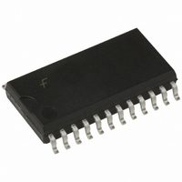
FAN5059MX Fairchild Semiconductor, FAN5059MX Datasheet - Page 13

FAN5059MX
Manufacturer Part Number
FAN5059MX
Description
IC CTRLR DC/DC PROG SYNC 24SOIC
Manufacturer
Fairchild Semiconductor
Datasheet
1.FAN5059MX.pdf
(18 pages)
Specifications of FAN5059MX
Applications
Controller, VRM8.5
Voltage - Input
5V
Number Of Outputs
1
Voltage - Output
1.3 ~ 3.5 V
Operating Temperature
0°C ~ 70°C
Mounting Type
Surface Mount
Package / Case
24-SOIC (7.5mm Width)
Output Current
18 A
Input Voltage
5 V
Mounting Style
SMD/SMT
Lead Free Status / RoHS Status
Lead free / RoHS Compliant
Other names
FAN5059MXTR
FAN5059MX_NL
FAN5059MX_NLTR
FAN5059MX_NLTR
FAN5059MX_NL
FAN5059MX_NLTR
FAN5059MX_NLTR
Available stocks
Company
Part Number
Manufacturer
Quantity
Price
Company:
Part Number:
FAN5059MX
Manufacturer:
MITEL
Quantity:
500
Part Number:
FAN5059MX
Manufacturer:
FAIRCHILD/ن»™ç«¥
Quantity:
20 000
PRODUCT SPECIFICATION
The softstart ramp begins at T(0) where UVLO is released.
During the period of t
switching is not enabled and thus the duty cycle is zero
(D=0) and the output voltage is zero. During t
cycle increased progressively from 0 to 1. This period is
where the output voltage ramps, dependent on output capaci-
tance and output load. If the duration of t
the output voltage will fully ramp to the point of regulation.
During t
effect on the output voltage.
NOTE: If a very large output capacitor bank is used it may
be required to use a larger C
ramp within t
Over-Voltage Protection
The FAN5059 constantly monitors the output voltage for pro-
tection against over-voltage conditions. If the voltage at the
VFB pin exceeds the selected program voltage, an over-volt-
age condition is assumed and the FAN5059 disables the out-
put drive signal to the external high-side MOSFET. The DC-
DC converter returns to normal operation after the output
voltage returns to normal levels.
Oscillator
The FAN5059 oscillator section uses a fixed frequency of
operation of 300KHz.
Design Considerations and Component
Selection
Additional information on design and component selection
may be found in Fairchild’s Application Note 57.
MOSFET Selection
This application requires N-channel Logic Level Enhancement
Mode Field Effect Transistors. Desired characteristics are as
follows:
• Low Static Drain-Source On-Resistance, R
• Low gate drive voltage, V
• Power package with low Thermal Resistance
• Drain-Source voltage rating > 15V.
The on-resistance (R
MOSFET selection. The on-resistance determines the power
dissipation within the MOSFET and therefore significantly
REV. 1.0.4 8/14/03
(lower is better)
V
SS
3
the softstart pin continues to ramp but without
2.75V
2.25V
5V
2
.
T(0)
DS,ON)
1
t
the softstart pin ramps but the PWM
1
SS
is the primary parameter for
GS
T
to ensure a full output voltage
t
2
= 4.5V rated
t
3
2
is long enough
DS,ON
2
the duty
< 20m
affects the efficiency of the DC-DC Converter. For details
and a spreadsheet on MOSFET selection, refer to Applica-
tions Bulletin AB-8.
Inductor Selection
Choosing the value of the inductor is a tradeoff between
allowable ripple voltage and required transient response. The
system designer can choose any value within the allowed
minimum to maximum range in order to either minimize ripple
or maximize transient performance. The first order equation
(close approximation) for minimum inductance is:
where:
V
V
f = DC/DC converter switching frequency
ESR = Equivalent series resistance of all output capacitors in
parallel
V
The first order equation for maximum allowed inductance is:
where:
C
I
V
transient
D
95%).
Some margin should be maintained away from both L
L
expense since all the variables are predetermined by system
performance except for C
increase L. Adding margin by decreasing L can be done by
purchasing capacitors with lower ESR. The FAN5059
provides significant cost savings for the newer CPU systems
that typically run at high supply current.
FAN5059 Short Circuit Current Characteristics
The FAN5059 protects against output short circuit on the
core supply by turning off both the high-side and low-side
MOSFETs and resetting softstart. The short circuit limit is
set with the R
Note: R
than 10.8K allows, a FET with lower R
pp
out
max
in
o
ripple
tb
m
= The total output capacitance
= Maximum to minimum load transient current
= Input Power Supply
= The output voltage tolerance budget allocated to load
= Maximum duty cycle for the DC/DC converter (usually
= Output Voltage
. Adding margin by increasing L almost always adds
= Maximum peak to peak output ripple voltage budget.
L
S
min
cannot exceed 10.8K. If a higher current is required
L
max
=
S
R
resistor, as given by the formula
=
S
(V in – V
=
2C
O
f
O
I
SC
, which must be increased to
out
(V in – V
)
I
*R
Detect
I
DS, on
x
pp 2
out
V
V
) D
out
in
DSon
m
x
V
must be used.
tb
V
ESR
ripple
FAN5059
min
and
13


