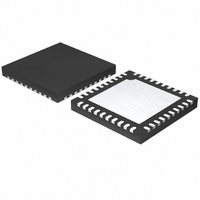
ISL6566CRZ-TR5184 Intersil, ISL6566CRZ-TR5184 Datasheet - Page 11

ISL6566CRZ-TR5184
Manufacturer Part Number
ISL6566CRZ-TR5184
Description
IC CTRLR PWM 3PHASE BUCK 40-QFN
Manufacturer
Intersil
Datasheet
1.ISL6566CRZ-TR5184.pdf
(29 pages)
Specifications of ISL6566CRZ-TR5184
Applications
Controller, Intel VRM9, VRM10, and AMD Hammer Applications
Voltage - Input
3 ~ 12 V
Number Of Outputs
1
Voltage - Output
0.84 ~ 1.6 V
Operating Temperature
0°C ~ 70°C
Mounting Type
Surface Mount
Package / Case
40-VFQFN, 40-VFQFPN
Rohs Compliant
YES
Lead Free Status / RoHS Status
Lead free / RoHS Compliant
Other names
ISL6566CRZ-TR5184
ISL6566CRZ-TR5184TR
ISL6566CRZ-TR5184TR
Figures 22 and 23 in the section entitled Input Capacitor
Selection can be used to determine the input-capacitor RMS
current based on load current, duty cycle, and the number of
channels. They are provided as aids in determining the
optimal input capacitor solution.
PWM Operation
The timing of each converter leg is set by the number of
active channels. The default channel setting for the ISL6566
is three. One switching cycle is defined as the time between
the internal PWM1 pulse termination signals. The pulse
termination signal is the internally generated clock signal
that triggers the falling edge of PWM1. The cycle time of the
pulse termination signal is the inverse of the switching
frequency set by the resistor between the FS pin and
ground. Each cycle begins when the clock signal commands
PWM1 to go low. The PWM1 transition signals the internal
channel-1 MOSFET driver to turn off the channel-1 upper
MOSFET and turn on the channel-1 synchronous MOSFET.
In the default channel configuration, the PWM2 pulse
terminates 1/3 of a cycle after the PWM1 pulse. The PWM3
pulse terminates 1/3 of a cycle after PWM2.
If PVCC3 is left open or connected to ground, two channel
operation is selected and the PWM2 pulse terminates 1/2 of
a cycle after the PWM1 pulse terminates. If both PVCC3 and
PVCC2 are left open or connected to ground, single channel
operation is selected.
Once a PWM pulse transitions low, it is held low for a
minimum of 1/3 cycle. This forced off time is required to
ensure an accurate current sample. Current sensing is
described in the next section. After the forced off time
expires, the PWM output is enabled. The PWM output state
is driven by the position of the error amplifier output signal,
V
sawtooth ramp as illustrated in Figure 3. When the modified
V
transitions high. The internal MOSFET driver detects the
change in state of the PWM signal and turns off the
synchronous MOSFET and turns on the upper MOSFET.
The PWM signal will remain high until the pulse termination
signal marks the beginning of the next cycle by triggering the
PWM signal low.
Channel-Current Balance
One important benefit of multi-phase operation is the thermal
advantage gained by distributing the dissipated heat over
multiple devices and greater area. By doing this the designer
avoids the complexity of driving parallel MOSFETs and the
expense of using expensive heat sinks and exotic magnetic
materials.
In order to realize the thermal advantage, it is important that
each channel in a multi-phase converter be controlled to
carry about the same amount of current at any load level. To
achieve this, the currents through each channel must be
sampled every switching cycle. The sampled currents, I
COMP
COMP
, minus the current correction signal relative to the
voltage crosses the sawtooth ramp, the PWM output
11
n
,
ISL6566
ISL6566
from each active channel are summed together and divided
by the number of active channels. The resulting cycle
average current, I
current demand on the converter during each switching
cycle. Channel-current balance is achieved by comparing
the sampled current of each channel to the cycle average
current, and making the proper adjustment to each channel
pulse width based on the error. Intersil’s patented current-
balance method is illustrated in Figure 3, with error
correction for channel 1 represented. In the figure, the cycle
average current, I
sample, I
The filtered error signal modifies the pulse width
commanded by V
I
correction is applied to each active channel.
Current Sampling
In order to realize proper current-balance, the currents in
each channel must be sampled every switching cycle. This
sampling occurs during the forced off-time, following a PWM
transition low. During this time the current-sense amplifier
uses the ISEN inputs to reproduce a signal proportional to
the inductor current, I
a scaled version of the inductor current. The sample window
opens exactly 1/6 of the switching period, t
PWM transitions low. The sample window then stays open
the rest of the switching cycle until PWM transitions high
again, as illustrated in Figure 4.
The sampled current, at the end of the t
proportional to the inductor current and is held until the next
switching period sample. The sampled current is used only
for channel-current balance.
ER
NOTE: Channel 2 and 3 are optional.
FIGURE 3. CHANNEL-1 PWM FUNCTION AND CURRENT-
toward zero. The same method for error signal
V
COMP
1
, to create an error signal I
FILTER
BALANCE ADJUSTMENT
+
I
ER
COMP
AVG
AVG
-
+
f(s)
I
1
L
, provides a measure of the total load-
, is compared with the channel 1
-
. This sensed current, I
I
AVG
to correct any unbalance and force
SAWTOOTH SIGNAL
÷ N
+
-
ER
PWM1
.
SAMPLE
Σ
SW
SEN
, after the
, is
CONTROL
TO GATE
, is simply
LOGIC
I
I
March 9, 2006
3
2
FN9178.4


