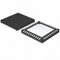
ISL6566CRZ-TR5184 Intersil, ISL6566CRZ-TR5184 Datasheet - Page 22

ISL6566CRZ-TR5184
Manufacturer Part Number
ISL6566CRZ-TR5184
Description
IC CTRLR PWM 3PHASE BUCK 40-QFN
Manufacturer
Intersil
Datasheet
1.ISL6566CRZ-TR5184.pdf
(29 pages)
Specifications of ISL6566CRZ-TR5184
Applications
Controller, Intel VRM9, VRM10, and AMD Hammer Applications
Voltage - Input
3 ~ 12 V
Number Of Outputs
1
Voltage - Output
0.84 ~ 1.6 V
Operating Temperature
0°C ~ 70°C
Mounting Type
Surface Mount
Package / Case
40-VFQFN, 40-VFQFPN
Rohs Compliant
YES
Lead Free Status / RoHS Status
Lead free / RoHS Compliant
Other names
ISL6566CRZ-TR5184
ISL6566CRZ-TR5184TR
ISL6566CRZ-TR5184TR
The total gate drive power losses are dissipated among the
resistive components along the transition path and in the
bootstrap diode. The portion of the total power dissipated in
the controller itself is the power dissipated in the upper drive
path resistance, P
P
power will be dissipated by the external gate resistors (R
and R
the MOSFETs. Figures 15 and 16 show the typical upper
and lower gate drives turn-on transition path. The total power
dissipation in the controller itself, P
estimated as:
Current Balancing Component Selection
The ISL6566 senses the channel load current by sampling
the voltage across the lower MOSFET r
Figure 17. The ISEN pins are denoted ISEN1, ISEN2, and
ISEN3. The resistors connected between these pins and the
respective phase nodes determine the gains in the channel-
current balance loop.
P
P
P
R
P
DR_UP
FIGURE 16. TYPICAL LOWER-GATE DRIVE TURN-ON PATH
DR
DR_UP
DR_LOW
EXT1
BOOT
PVCC
=
G2
P
=
, and in the boot strap diode, P
=
) and the internal gate resistors (R
R
DR_UP
=
R
R
LO2
=
P
---------------------
HI2
G1
Qg_Q1
--------------------------------------
R
HI1
--------------------------------------
R
3
+
HI2
+
R
-------------
R
N
+
P
GI1
DR_UP
HI1
Q1
R
R
+
DR_LOW
LGATE
HI2
EXT1
R
EXT2
, the lower drive path resistance,
+
+
--------------------------------------- -
R
+
22
LO1
--------------------------------------- -
R
P
R
R
LO2
G2
BOOT
EXT2
R
G
+
LO1
R
+
DR
R
LO2
R
C
EXT1
R
GI2
GD
+
=
, can be roughly
C
EXT2
(
BOOT
R
GS
I
DS(ON)
Q
G2
•
•
GI1
S
VCC
+
. The rest of the
P
---------------------
•
R
-------------
Qg_Q1
N
P
---------------------
GI2
, as shown in
and R
Q2
Qg_Q2
D
3
)
2
Q2
C
DS
(EQ. 23)
GI2
) of
G1
ISL6566
Select values for these resistors based on the room
temperature r
operating current, I
Equation 24.
In certain circumstances, it may be necessary to adjust the
value of one or more ISEN resistors. When the components of
one or more channels are inhibited from effectively dissipating
their heat so that the affected channels run hotter than
desired, choose new, smaller values of R
phases (see the section entitled Channel-Current Balance).
Choose R
temperature rise in order to cause proportionally less current
to flow in the hotter phase.
In Equation 25, make sure that ∆T
rise above the ambient temperature, and ∆T
temperature rise above the ambient temperature. While a
single adjustment according to Equation 25 is usually
sufficient, it may occasionally be necessary to adjust R
two or more times to achieve optimal thermal balance
between all channels.
Load Line Regulation Component Selection (DCR
Current Sensing)
For accurate load line regulation, the ISL6566 senses the
total output current by detecting the voltage across the
output inductor DCR of each channel (As described in the
Load Line Regulation section). As Figure 18 illustrates, an
R-C network is required to accurately sense the inductor
DCR voltage and convert this information into a “droop”
voltage, which is proportional to the total output current.
Choosing the components for this current sense network is a
two step process. First, R
chosen so that the time constant of this R
network matches the time constant of the inductor L/DCR.
R
R
FIGURE 17. ISL6566 INTERNAL AND EXTERNAL CURRENT-
ISEN
ISEN 2 ,
ISL6566
=
=
---------------------- -
50 10
r
ISEN,2
DS ON
R
×
ISEN
(
SENSING CIRCUITRY
DS(ON)
–
6
)
in proportion to the desired decrease in
ISEN(n)
∆T
----------
∆T
I
------- -
FL
FL
N
CHANNEL N
LOWER MOSFET
2
1
; and the number of phases, N using
of the lower MOSFETs; the full-load
R
ISEN
COMP
V
IN
and C
+
2
CHANNEL N
UPPER MOSFET
-
I
L
is the desired temperature
r
DS ON
I
COMP
L
(
ISEN
COMP
1
)
is the measured
must be
for the affected
-C
COMP
March 9, 2006
(EQ. 24)
(EQ. 25)
ISEN
FN9178.4


