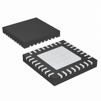
MAX1585ETJ+ Maxim Integrated Products, MAX1585ETJ+ Datasheet - Page 12

MAX1585ETJ+
Manufacturer Part Number
MAX1585ETJ+
Description
IC DGTL CAM PWR SUP 5CH 32TQFN
Manufacturer
Maxim Integrated Products
Datasheet
1.MAX1585ETJ.pdf
(29 pages)
Specifications of MAX1585ETJ+
Applications
Controller, Digital Camera
Voltage - Input
0.7 ~ 5.5 V
Number Of Outputs
5
Voltage - Output
1.25 ~ 5.5 V
Operating Temperature
-40°C ~ 85°C
Mounting Type
Surface Mount
Package / Case
32-TQFN Exposed Pad
Lead Free Status / RoHS Status
Lead free / RoHS Compliant
The MAX1584/MAX1585 are complete power-conver-
sion ICs for slim digital still cameras. They can accept
input from a variety of sources, including single-cell Li+
batteries and 2-cell alkaline or NiMH batteries, as well
as systems designed to accept both battery types. The
MAX1584/MAX1585 include five DC-DC converter
channels to generate all required voltages (Figure 2
shows a functional diagram):
• Synchronous-rectified step-up DC-DC converter with
• Synchronous-rectified step-down DC-DC converter
• AUX1 step-up controller—Typically used for 15V to
5-Channel Slim DSC Power Supplies
12
PAD
PIN
on-chip MOSFETs—Typically supplies 3.3V for main
system power or 5V to power other DC-DC convert-
ers for boost-buck designs.
with on-chip MOSFETs—Typically supplies 1.8V for
the DSP core. Powering the step-down from the
step-up output provides efficient (up to 90%) boost-
buck functionality that supplies a regulated output
when the battery voltage is above or below the out-
put voltage. The step-down can also be powered
from the battery if there is sufficient headroom.
bias one or more of the LCD, CCD, and LED back-
lights.
28
29
30
31
32
______________________________________________________________________________________
NAME
GND
CC3
DL3
DL1
FB3
EP
Detailed Description
AUX3 Step-Down Controller Gate-Drive Output. Connect to the gate of a P-channel MOSFET. DL3 swings
from GND to PVSU and supplies up to 500mA. DL3 is driven to PVSU in shutdown and thermal limit.
AUX1 Step-Up Controller Gate-Drive Output. Connect to the gate of an N-channel MOSFET. DL1 swings
from GND to PVSU and supplies up to 500mA. DL1 is driven to GND in shutdown and thermal limit.
Analog Ground. Connect to all PG_ pins as close to the IC as possible.
AUX3 Step-Down Controller Compensation Node. Connect a series resistor-capacitor from CC3 to FB3 to
compensate the converter control loop. This pin is actively driven to GND in shutdown, overload, and
thermal limit. See the AUX Compensation section.
PWM Step-Up Controller 3 Feedback Input. Connect a resistive voltage-divider from the output voltage to
FB3 to GND to set the output voltage. The FB3 feedback threshold is 1.25V. This pin is high impedance in
shutdown.
Exposed Underside Metal Pad. This pad must be soldered to the PC board to achieve package thermal
and mechanical ratings. There is no internal metal or bond wire physically connecting the exposed pad to
the GND pin(s). Connecting the exposed pad to ground does not remove the requirement for a good
ground connection to the appropriate IC pins.
• AUX2 step-up controller (MAX1584)—Typically sup-
• AUX2 inverter controller (MAX1585)—Typically sup-
• AUX3 step-down controller—Typically steps 5V gen-
The step-up DC-DC switching converter is typically used
to generate a 5V output voltage from a 1.5V to 4.5V bat-
tery input, but any voltage from V
internal NFET switch and a PFET synchronous rectifier
allow conversion efficiencies as high as 95%. Under
moderate to heavy loading, the converter operates in a
low-noise PWM mode with constant frequency and modu-
lated pulse width. Switching harmonics generated by
fixed-frequency operation are consistent and easily fil-
tered. Efficiency is enhanced under light (<75mA typ)
loading, by an idle mode that switches the step-up only
as needed to service the load. In this mode, the maxi-
mum inductor current is 250mA for each pulse.
plies remaining bias voltages with either a multi-out-
put flyback transformer or a boost converter with
charge-pump inverter. Alternately, can power white
LEDs for LCD backlighting.
plies negative CCD bias when high current is need-
ed for large pixel-count CCDs.
erated at PVSU down to 3.3V for system logic in
boost-buck designs.
FUNCTION
Pin Description (continued)
Step-Up DC-DC Converter
IN
to 5V can be set. An


