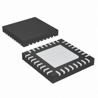
MAX1585ETJ+ Maxim Integrated Products, MAX1585ETJ+ Datasheet - Page 21

MAX1585ETJ+
Manufacturer Part Number
MAX1585ETJ+
Description
IC DGTL CAM PWR SUP 5CH 32TQFN
Manufacturer
Maxim Integrated Products
Datasheet
1.MAX1585ETJ.pdf
(29 pages)
Specifications of MAX1585ETJ+
Applications
Controller, Digital Camera
Voltage - Input
0.7 ~ 5.5 V
Number Of Outputs
5
Voltage - Output
1.25 ~ 5.5 V
Operating Temperature
-40°C ~ 85°C
Mounting Type
Surface Mount
Package / Case
32-TQFN Exposed Pad
Lead Free Status / RoHS Status
Lead free / RoHS Compliant
If Z
with ceramic output capacitors. If Z
it should be cancelled with a pole set by capacitor C
connected from CCSU to GND:
If C
The external components required for the step-down
are an inductor, input and output filter capacitors, and
a compensation RC network.
The MAX1585/1585 step-down converter provides best
efficiency with continuous inductor current. A reason-
able inductor value (L
following:
which sets the peak-to-peak inductor current at half the
DC inductor current. D is the duty cycle:
Given L
I
Inductance values smaller than L
reduce inductor size; however, if much smaller values
are used, inductor current rises and a larger output
capacitance may be required to suppress output ripple.
Larger values than L
output current, but with typically larger inductor size.
The relevant characteristics for step-down compensa-
tion are as follows:
• Transconductance (from FBSD to CCSD), g
• Current-sense amplifier transresistance, R
• Feedback regulation voltage, V
• Step-down output voltage, V
• Output load equivalent resistance, R
The key steps for step-down compensation are as fol-
lows:
1) Set the compensation RC zero to cancel the R
2) Set the loop crossover below 1/10 the switching fre-
If we assume V
250mA, then R
If we select f
OUT
(135µS)
Ω = V
C
quency.
ESR
P
. The absolute peak inductor current is 1.25 x I
OUT
is calculated to be <10pF, it can be omitted.
L
IDEAL
> f
IDEAL
SD
pole.
C
/ I
, it can be ignored, as is typically the case
OSC
Step-Down Component Selection
, the peak-to-peak inductor current is 0.5 x
LOAD
= [2(V
LOAD
C
IN
= 500kHz and L = 22µH,
P
______________________________________________________________________________________
= C
= 3.5V, V
D = V
IDEAL
= 6Ω.
IN
IDEAL
) x D(1 - D)] / I
OUT
OUT
can be used to obtain higher
Step-Down Compensation
x R
) can be derived from the
5-Channel Slim DSC Power Supplies
OUT
/ V
ESR
SD
IN
IDEAL
, in V
Step-Down Inductor
FB
= 1.5V, and I
/ R
ESR
OUT
(1.25V)
C
can be used to
is less than f
x f
CS
OSC
LOAD
(0.6V/A)
OUT
LOAD
OUT
MEA
, in
C
=
P
,
.
choose f
Choose 4.7nF.
Now select R
For example, if 4% transient droop is allowed, the input
to the error amplifier moves 0.04 x 1.25V, or 50mV. The
error-amp output drives 50mV x 135µS, or 6.75µA across
R
transresistance is 0.6V/A, the value of R
required load step swing is as follows:
In a step-down DC-DC converter, If L
put current relates to inductor current by the following:
So for a 250mA output load step with V
V
Choose 27kΩ.
The inductor does somewhat limit the response in this
case since it ramps at (V
/ 22µH = 90mA/µs.
The output filter capacitor is then chosen so the C
R
For the example:
Choose 22µF or greater.
If the output filter capacitor has significant ESR, a zero
occurs at:
If Z
with ceramic output capacitors. If Z
it should be cancelled with a pole set by capacitor C
connected from CCSD to GND:
If C
MAX1584/MAX1585 AUX1(step-up) controllers drive
external logic-level N-channel MOSFETs. AUX3 (step-
down) controllers drive P-channel MOSFETs. AUX2
(step-up) on the MAX1584 drives an N channel, while
AUX2 (inverting) on the MAX1585 drives a P channel.
OUT
C
LOAD
ESR
P
C
to provide transient gain. Since the current-sense
C
is calculated to be <10pF, it can be omitted.
= 1.5V:
R
= (V
= (1.25 / 1.5)(6 / 0.6) x (135µS / (6.28 x 40kHz))
= 4.5nF
pole cancels the R
AUX Controller Component Selection
> f
C
C
= (1.25 x 0.6 x 0.25) / 6.75µA = 27.8kΩ
= 24kHz and calculate C
C
C
FB
, it can be ignored, as is typically the case
OUT
Z
C
R
ESR
/ V
C
so transient-droop requirements are met.
C
C
OUT
OUT
I
= 27kΩ x 4.7nF / 6Ω = 21µF
= 0.6 x I
IND(PK)
P
= 1 / (2π x C
= C
)(R
x R
OUT
LOAD
LOAD
IN
= 1.25 x I
IND(PK)
C
- V
x R
C
C
/ R
OUT
= R
OUT
ESR
zero:
CS
/ 6.75µA
C
) / 22µH, or (3.5 - 1.5)
OUT
)(g
C
x R
/ R
x C
ESR
External MOSFET
:
IDEAL
M
C
ESR
C
C
/ 2π x f
is less than f
IN
that allows the
)
is used, out-
= 3.5V and
C
)
OUT
21
C
P
,


