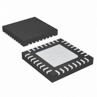
MAX1585ETJ+ Maxim Integrated Products, MAX1585ETJ+ Datasheet - Page 20

MAX1585ETJ+
Manufacturer Part Number
MAX1585ETJ+
Description
IC DGTL CAM PWR SUP 5CH 32TQFN
Manufacturer
Maxim Integrated Products
Datasheet
1.MAX1585ETJ.pdf
(29 pages)
Specifications of MAX1585ETJ+
Applications
Controller, Digital Camera
Voltage - Input
0.7 ~ 5.5 V
Number Of Outputs
5
Voltage - Output
1.25 ~ 5.5 V
Operating Temperature
-40°C ~ 85°C
Mounting Type
Surface Mount
Package / Case
32-TQFN Exposed Pad
Lead Free Status / RoHS Status
Lead free / RoHS Compliant
Inductance values smaller than L
reduce inductor size; however, if much smaller values are
used, inductor current rises and a larger output capaci-
tance might be required to suppress output ripple.
The inductor and output capacitor are usually chosen
first in consideration of performance, size, and cost.
The compensation resistor and capacitor are then cho-
sen to optimize control-loop stability. In some cases, it
helps to readjust the inductor or output capacitor value
to get optimum results. For typical designs, the compo-
nent values in the circuit of Figure 1 yield good results.
The step-up converter employs current-mode control,
thereby simplifying the control-loop compensation.
When the converter operates with continuous inductor
current (typically the case), a right-half-plane zero
appears in the loop-gain frequency response. To
ensure stability, the control-loop gain should cross over
(drop below unity gain) at a frequency (f
than that of the right-half-plane zero.
The relevant characteristics for step-up channel com-
pensation are as follows:
• Transconductance (from FBSU to CCSU), g
• Current-sense amplifier transresistance, R
• Feedback regulation voltage, V
• Step-up output voltage, V
• Output load equivalent resistance, R
The key steps for step-up compensation are as follows:
1) Place f
2) Select R
3) Calculate the output-filter capacitor (C
4) Determine if C
5-Channel Slim DSC Power Supplies
20
(135µS)
(0.3V/A)
Ω = V
(RHPZ) and calculate C
R
sponds to load-current step.
to allow the R
C
______________________________________________________________________________________
sets a voltage delta on the C
SUOUT
C
C
sufficiently below the right-half-plane zero
I
IND(PK)
based on the allowed load-step transient.
/ I
C
P
LOAD
is required (if calculated to be >10pF).
and C
= 1.25 x I
C
selected.
C
.
SU
OUT
Step-Up Compensation
, in V
IDEAL
FB
/ (1 - D)
(1.25V)
C
can be used to
pin that corre-
OUT
C
) much less
) required
LOAD
MEA
, in
CS
For continuous conduction, the right-half-plane zero fre-
quency (f
where D = the duty cycle = 1 - (V
inductor value, and I
rent. Typically, target crossover (f
RHPZ. For example, if we assume f
= 2.5V, V
10Ω. If we select L = 4.7µH, then:
Choose f
C
Choose 6.8nF.
Now select R
met. As an example, if 4% transient droop is allowed,
the input to the error amplifier moves 0.04 x 1.25V, or
50mV. The error-amp output drives 50mV x 135µS, or
6.75µA across R
current-sense transresistance is 0.3V/A, the value of R
that allows the required load step swing is as follows:
In a step-up DC-DC converter, if L
current relates to inductor current by:
So for a 500mA output load step with V
V
Note that the inductor does not limit the response in this
case since it can ramp at 2.5V / 4.7µH, or 530mA/µs.
The output filter capacitor is then chosen so the C
R
For the example:
Choose 47µF for C
stantially different from the calculated value, insert the
available C
recalculate R
higher R
consequently less transient droop.
If the output filter capacitor has significant ESR, a zero
occurs at the following:
f
I
RHPZ
OUT
LOAD
C
IND(PK)
= (V
= (1.25 / 5)(10 / 0.3) x (135µS / (6.28 x 14kHz) (2/5)
= 6.4nF
R
C
= 5V:
f
= 5 (2.5 / 5)
= [1.25(0.3 x 0.5 x 5) / 2)] / 6.75µA = 69.4kΩ
pole cancels the R
RHPZ
FB
C
C
RHPZ
= 1.25 x I
OUT
C
, which provides higher transient gain and
/ V
= 14kHz. Calculate C
V
OUT
OUT
Z
= V
IN
C
OUT
ESR
) is given by the following:
C
. Higher substituted C
= 5V, and I
R
C
C
= 68kΩ x 6.8nF / 10Ω = 46µF
OUT
SUOUT
so transient-droop requirements are
C
)(R
value into the above equation and
= 1 / (2π x C
= 0.3 I
2
OUT
to provide transient gain. Since the
OUT
/ (2π x 4.7 x 10
LOAD
LOAD
x R
/ (1 - D) = 1.25 x I
(1 - D)
. If the available C
LOAD
IND(PK)
C
/ R
OUT
is the maximum output cur-
C
CS
C
2
= R
OUT
)(g
/ (2π x L x I
zero:
= 0.5A, then R
C
/ 6.75µA
:
C
M
IDEAL
-6
x R
IN
x C
OSC
/ 2π x f
OUT
x 0.5) = 84.65kHz
C
ESR
/ V
C
) for 1/6 of the
is used, output
= 500kHz, V
OUT
IN
OUT
values allow a
)
LOAD
C
OUT
= 2.5V and
)(1 - D)
), L is the
x V
LOAD
)
is sub-
OUT
OUT
/
IN
=
C


