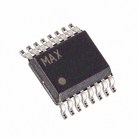
MAX1809EEE+ Maxim Integrated Products, MAX1809EEE+ Datasheet

MAX1809EEE+
Specifications of MAX1809EEE+
Related parts for MAX1809EEE+
MAX1809EEE+ Summary of contents
Page 1
... FB SHDN V SET EXTREF REF TOFF SS ________________________________________________________________ Maxim Integrated Products For pricing, delivery, and ordering information, please contact Maxim/Dallas Direct! at 1-888-629-4642, or visit Maxim’s website at www.maxim-ic.com. o Source/Sink 3A o ±1% Output Accuracy 1MHz Switching Frequency o 93% Efficiency o Internal PMOS/NMOS Switches 90mΩ/70mΩ On-Resistance at V 110mΩ ...
Page 2
DDR Memory Termination Supply ABSOLUTE MAXIMUM RATINGS GND ........................................................-0. .............................................................................±0.3V CC GND to PGND.....................................................................±0.3V SHDN, SS, FB OFF REF EXTREF to GND.......................................-0. ...
Page 3
DDR Memory Termination Supply ELECTRICAL CHARACTERISTICS (continued 3.3V 1.1V EXTREF A PARAMETER SYMBOL SS Source Current SS Sink Current SHDN Input Current SHDN Logic Levels Maximum Output RMS Current ...
Page 4
DDR Memory Termination Supply (Circuit of Figure 1.25V, for V OUT IN EFFICIENCY vs. OUTPUT CURRENT (SOURCING) 100 R = 0Ω DROOP 5V 2.5V 75 OUT ...
Page 5
DDR Memory Termination Supply (Circuit of Figure 1.25V, for V OUT LOAD-TRANSIENT RESPONSE 0V 0A 10µs/div V = 1.25V 3.3V, I EXTREF IN OUT SWITCHING WAVEFORMS (SOURCING 400ns/div I = 2A, ...
Page 6
DDR Memory Termination Supply PIN (QFN) PIN (QSOP 10, 11, 12, — 22, 24, 26 18, 19 ...
Page 7
DDR Memory Termination Supply V 10Ω 2.2µF V DDQ (2.5V) 10kΩ 10kΩ V SSQ Figure 1. Typical Application Circuit feedback voltage exceeds the external reference voltage ( the positive current limit is reached. When EXTREF the ...
Page 8
DDR Memory Termination Supply where C = 2.5nF and f is the switching frequency. SW Resistive losses in the two power switches are approxi- mated by: 2 ✕ D(RES) OUT PMOS where R is ...
Page 9
DDR Memory Termination Supply SOURCE SYNCHRONOUS BUCK MODE (SOURCING CURRENT SINK SYNCHRONOUS BOOST MODE (SINKING CURRENT) Figure 3. Sourcing and Sinking Capabilities of the MAX1809 Programming the Switching Frequency and Off-Time and ...
Page 10
DDR Memory Termination Supply to maximum DC load current. A higher value of LIR allows smaller inductance but results in higher losses and ripple. A good compromise between size and losses is found at approximately a 25% ripple ...
Page 11
DDR Memory Termination Supply LX V DDQ MAX1809 V EXTREF FB EXTREF (1.1V ≤ V ≤ 1.7V) EXTREF IN Figure 5. Adjusting the Output Voltage Using EXTREF The output current limit during soft-start varies with the ...
Page 12
DDR Memory Termination Supply output regulates at a slightly lower voltage under a given load, allowing more voltage headroom as the load changes suddenly to zero or to the opposite polarity (sinking mode). By utilizing the full-voltage tolerance ...
Page 13
DDR Memory Termination Supply INPUT VOLTAGE (3V TO 5.5V 10Ω 2.2µF SHDN SHDN Figure 9. Discharging the Output of the MAX1809 in Shutdown INPUT VOLTAGE (3V TO 5.5V ...
Page 14
DDR Memory Termination Supply before startup, a 100Ω resistor should be added in the feedback path, and a diode from shown in Figure 10. SS will keep FB low during the startup sequence, ensuring ...
Page 15
DDR Memory Termination Supply (The package drawing(s) in this data sheet may not reflect the most current specifications. For the latest package outline information www.maxim-ic.com/packages.) ______________________________________________________________________________________ Package Information (continued) 15 ...
Page 16
DDR Memory Termination Supply (The package drawing(s) in this data sheet may not reflect the most current specifications. For the latest package outline information www.maxim-ic.com/packages.) 16 ______________________________________________________________________________________ Package Information (continued) ...
Page 17
... Maxim cannot assume responsibility for use of any circuitry other than circuitry entirely embodied in a Maxim product. No circuit patent licenses are implied. Maxim reserves the right to change the circuitry and specifications without notice at any time. Maxim Integrated Products, 120 San Gabriel Drive, Sunnyvale, CA 94086 408-737-7600 ____________________ 17 © 2002 Maxim Integrated Products ...


