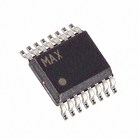
MAX1809EEE+ Maxim Integrated Products, MAX1809EEE+ Datasheet - Page 6

MAX1809EEE+
Manufacturer Part Number
MAX1809EEE+
Description
IC DDR TERMINATION 16-QSOP
Manufacturer
Maxim Integrated Products
Datasheet
1.MAX1809EEE.pdf
(17 pages)
Specifications of MAX1809EEE+
Applications
Converter, DDR
Voltage - Input
3 ~ 5.5 V
Number Of Outputs
1
Voltage - Output
1.1 ~ 5.5 V
Operating Temperature
0°C ~ 85°C
Mounting Type
Surface Mount
Package / Case
16-QSOP
Lead Free Status / RoHS Status
Lead free / RoHS Compliant
3A, 1MHz, DDR Memory Termination Supply
The MAX1809 synchronous, current-mode, constant-
off-time, PWM DC-DC converter steps down input volt-
ages of 3V to 5.5V to an adjustable output voltage from
1.1V to V
sources and sinks up to 3A of output current. Internal
switches composed of a 90mΩ PMOS power switch
and a 70mΩ NMOS synchronous-rectifier switch
improve efficiency, reduce component count, and elim-
inate the need for an external Schottky diode across
the synchronous switch.
The MAX1809 operates in a constant-off-time mode
under all loads. A single resistor-programmable con-
stant-off-time control sets switching frequencies up to
1MHz, allowing the user to optimize performance trade-
6
13, backside pad,
3, 18, 19, 23, 25
1, 5, 10, 11, 12,
_______________________________________________________________________________________
22, 24, 26, 28
corner tabs
PIN (QFN)
17, 20, 21
2, 4
14
15
16
27
IN
6
7
8
9
, as set by the voltage applied at EXTREF. It
PIN (QSOP)
Detailed Description
3, 14, 16
13, 15
2, 4
—
10
11
12
5
6
7
8
9
1
EXTREF
NAME
PGND
SHDN
TOFF
GND
GND
N.C.
REF
V
SS
FB
LX
IN
CC
No Connection. Not internally connected.
Supply Voltage Input for the Internal PMOS Power Switch. Not internally
connected. Externally connect all pins for proper operation.
Inductor Connection. Connection for the drains of the PMOS power switch
and NMOS synchronous-rectifier switch. Connect the inductor from this
node to the output filter capacitor and load. Not internally connected.
Externally connect all pins for proper operation.
Soft-Start. Connect a capacitor from SS to GND to limit inrush current
during startup.
External Reference Input. Feedback input regulates to V
controller remains off until EXTREF is greater than REF.
Off-Time Select Input. Sets the PMOS power switch constant-off-time.
Connect a resistor from TOFF to GND to adjust the PMOS switch off-time.
Feedback Input. Connect directly to output for fixed-voltage operation or to
a resistive-divider for adjustable operating modes.
Analog Ground. Connect exposed backside pad and corner tabs to analog
GND.
Reference Output. Bypass REF to GND with a 1µF capacitor.
Tie to GND (pin 13 QFN; pin 9 QSOP)
Analog Supply Voltage Input. Supplies internal analog circuitry. Bypass
V
Power Ground. Internally connected to the internal NMOS synchronous-
rectifier switch.
Shutdown Control Input. Drive SHDN low to disable the reference, control
circuitry, and internal MOSFETs. Drive high or connect to V
operation.
CC
with a 10Ω and 2.2µF low-pass filter (see Figure 1).
offs in efficiency, switching noise, component size, and
cost.
When power is drawn from a regulated supply, con-
stant-off-time PWM architecture essentially provides
constant-frequency operation. This architecture has the
inherent advantage of quick response to line and load
transients. The MAX1809’s current-mode, constant-off-
time PWM architecture regulates the output voltage by
changing the PMOS switch on-time relative to the con-
stant off-time.
In the constant-off-time architecture, the FB voltage
comparator turns the PMOS switch on at the end of
each off-time, keeping the device in continuous-con-
duction mode. The PMOS switch remains on until the
FUNCTION
Constant-Off-Time Operation
Pin Description
EXTREF
CC
for normal
. The PWM


