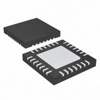
MAX8717ETI+ Maxim Integrated Products, MAX8717ETI+ Datasheet - Page 24

MAX8717ETI+
Manufacturer Part Number
MAX8717ETI+
Description
IC CNTRLR PWR SUP 28-TQFN
Manufacturer
Maxim Integrated Products
Datasheet
1.MAX8717ETI.pdf
(30 pages)
Specifications of MAX8717ETI+
Applications
Controller, Notebook Computers
Voltage - Input
4 ~ 26 V
Number Of Outputs
2
Voltage - Output
3.3V, 5V, 1 ~ 5.5 V
Operating Temperature
0°C ~ 85°C
Mounting Type
Surface Mount
Package / Case
28-TQFN Exposed Pad
Maximum Operating Temperature
+ 85 C
Mounting Style
SMD/SMT
Minimum Operating Temperature
- 40 C
Lead Free Status / RoHS Status
Lead free / RoHS Compliant
Interleaved High-Efficiency, Dual Power-Supply
Controllers for Notebook Computers
Stability is determined by the value of the ESR zero rel-
ative to the switching frequency. The boundary of insta-
bility is given by the following equation:
where:
For a typical 300kHz application, the ESR zero frequen-
cy must be well below 95kHz, preferably below 50kHz.
Tantalum and OS-CON capacitors in widespread use
at the time of publication have typical ESR zero fre-
quencies of 25kHz. In the design example used for
inductor selection, the ESR needed to support 25mV
ripple is 25mV/1.5A = 16.7mΩ. One 220µF/4V SANYO
polymer (TPE) capacitor provides 15mΩ (max) ESR.
This results in a zero at 48kHz, well within the bounds
of stability.
For low input-voltage applications where the duty cycle
exceeds 50% (V
voltage should not be greater than twice the internal
slope-compensation voltage:
where V
case ESR limit occurs when V
above equation can be simplified to provide the follow-
ing boundary condition:
Do not put high-value ceramic capacitors directly
across the feedback sense point without taking precau-
tions to ensure stability. Large ceramic capacitors can
have a high-ESR zero frequency and cause erratic,
unstable operation. However, it is easy to add enough
series resistance by placing the capacitors a couple of
inches downstream from the feedback sense point,
which should be as close as possible to the inductor.
Unstable operation manifests itself in two related but
distinctly different ways: short/long pulses or cycle
skipping resulting in a lower switching frequency.
Instability occurs due to noise on the output or because
the ESR is so low that there is not enough voltage ramp
in the output voltage signal. This “fools” the error com-
parator into triggering too early or skipping a cycle.
Cycle skipping is more annoying than harmful, resulting
in nothing worse than increased output ripple.
However, it can indicate the possible presence of loop
instability due to insufficient ESR. Loop instability can
result in oscillations at the output after line or load
steps. Such perturbations are usually damped, but can
24
______________________________________________________________________________________
RIPPLE
Output-Capacitor Stability Considerations
equals ΔI
R
V
OUT
ESR
ƒ
RIPPLE
ESR
≤ 0.04 x L x ƒ
/ V
ƒ
=
ESR
≤ 0.02 x V
2
INDUCTOR
IN
π
R
≤
≥ 50%), the output ripple
ESR OUT
ƒ
1
SW
π
IN
C
OUT
= 2 x V
OSC
x R
ESR
OUT
. The worst-
, so the
P-P
cause the output voltage to rise above or fall below the
tolerance limits.
The easiest method for checking stability is to apply a
very fast zero-to-max load transient and carefully
observe the output-voltage-ripple envelope for over-
shoot and ringing. It can help to simultaneously monitor
the inductor current with an AC current probe. Do not
allow more than one cycle of ringing after the initial
step-response under/overshoot.
The input capacitor must meet the ripple-current
requirement (I
For an out-of-phase regulator, the total RMS current in
the input capacitor is a function of the load currents,
the input currents, the duty cycles, and the amount of
overlap as defined in Figure 9.
The 40/60 optimal interleaved architecture of the
MAX8716/MAX8717/MAX8756/MAX8757 allows the
input voltage to go as low as 8.3V before the duty
cycles begin to overlap. This offers improved efficiency
over a regular 180° out-of-phase architecture where the
duty cycles begin to overlap below 10V. Figure 9
Figure 9. Input RMS Current
I
RMS
=
INPUT RMS CURRENT FOR INTERLEAVED OPERATION
INPUT RMS CURRENT FOR SINGLE-PHASE OPERATION
(I
(I
I
D
IN
I
OUT1
OUT1
RMS
LX1
5.0
4.5
4.0
3.5
3.0
2.5
2.0
1.5
1.0
0.5
=
0
=
V
= I
- I
+ I
OUT1
V
LOAD
RMS
6
IN
V
OUT2
OUT1
IN
)
2
50/50 INTERLEAVING
I
INPUT CAPACITOR RMS CURRENT
(D
OUT1
(
- I
LX1
V
IN
) imposed by the switching currents.
8
V
OUT
+ V
)
D
IN
- D
2
LX2
D
OUT2
(V
OL
OL
V
vs. INPUT VOLTAGE
=
IN
10
) + (I
IN
Input Capacitor Selection
+ I
V
- V
V
I
OUT2
OUT2
IN 2
IN
OUT
OUT2
IN PHASE
(1 - D
40/60 OPTIMAL
INTERLEAVING
12
)
V
- I
IN
)
IN
LX1
D
)
(V)
OL
2
14
(D
- D
= DUTY-CYCLE OVERLAP FRACTION
5V/5A AND 3.3V/5A
LX2
LX2
- D
+ D
16
OL
OL
) +
)
18
20


