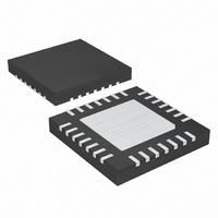
MAX8717ETI+ Maxim Integrated Products, MAX8717ETI+ Datasheet - Page 26

MAX8717ETI+
Manufacturer Part Number
MAX8717ETI+
Description
IC CNTRLR PWR SUP 28-TQFN
Manufacturer
Maxim Integrated Products
Datasheet
1.MAX8717ETI.pdf
(30 pages)
Specifications of MAX8717ETI+
Applications
Controller, Notebook Computers
Voltage - Input
4 ~ 26 V
Number Of Outputs
2
Voltage - Output
3.3V, 5V, 1 ~ 5.5 V
Operating Temperature
0°C ~ 85°C
Mounting Type
Surface Mount
Package / Case
28-TQFN Exposed Pad
Maximum Operating Temperature
+ 85 C
Mounting Style
SMD/SMT
Minimum Operating Temperature
- 40 C
Lead Free Status / RoHS Status
Lead free / RoHS Compliant
Interleaved High-Efficiency, Dual Power-Supply
Controllers for Notebook Computers
Choose a Schottky diode (D
drop low enough to prevent the low-side MOSFET’s
body diode from turning on during the dead time. As a
general rule, select a diode with a DC current rating
equal to 1/3 the load current. This diode is optional and
can be removed if efficiency is not critical.
The boost capacitors (C
enough to handle the gate-charging requirements of
the high-side MOSFETs. Typically, 0.1µF ceramic
capacitors work well for low-power applications driving
medium-sized MOSFETs. However, high-current appli-
cations driving large, high-side MOSFETs require boost
capacitors larger than 0.1µF. For these applications,
select the boost capacitors to avoid discharging the
capacitor more than 200mV while charging the high-
side MOSFETs’ gates:
where Q
high-side MOSFET’s data sheet. For example, assume
the FDS6612A n-channel MOSFET is used on the high
side. According to the manufacturer’s data sheet, a sin-
gle FDS6612A has a maximum gate charge of 13nC
(V
boost capacitance would be:
Selecting the closest standard value, this example
requires a 0.1µF ceramic capacitor.
The minimum input operating voltage (dropout voltage)
is restricted by the maximum duty-cycle specification
(see the Electrical Characteristics table). For the best
dropout performance, use the slowest switching-fre-
quency setting (FSEL = GND). However, keep in mind
that the transient performance gets worse as the step-
down regulators approach the dropout voltage, so bulk
output capacitance must be added (see the voltage
sag and soar equations in the Design Procedure sec-
tion). The absolute point of dropout occurs when the
inductor current ramps down during the off-time
(ΔI
26
GS
DOWN
______________________________________________________________________________________
= 5V). Using the above equation, the required
GATE
) as much as it ramps up during the on-time
is the total gate charge specified in the
C
Applications Information
BST
C
=
BST
100
13
BST
=
nC
mV
Q
200
) must be selected large
GATE
L
=
) with a forward-voltage
Minimum Input Voltage
mV
0 065
Duty-Cycle Limits
Boost Capacitors
.
μ
F
(ΔI
defined by the following equation:
where V
the charge and discharge paths, respectively. A rea-
sonable minimum value for h is 1.5, while the absolute
minimum input voltage is calculated with h = 1.
The MAX8716/MAX8717/MAX8756/MAX8757 controller
includes a minimum on-time specification, which deter-
mines the maximum input operating voltage that main-
tains the selected switching frequency (see the
Electrical Characteristics table). Operation above this
maximum input voltage results in pulse-skipping opera-
tion, regardless of the operating mode selected by
SKIP. At the beginning of each cycle, if the output volt-
age is still above the feedback threshold voltage, the
controller does not trigger an on-time pulse, effectively
skipping a cycle. This allows the controller to maintain
regulation above the maximum input voltage, but forces
the controller to effectively operate with a lower switch-
ing frequency. This results in an input threshold voltage
at which the controller begins to skip pulses (V
where f
Careful PCB layout is critical to achieving low switching
losses and clean, stable operation. The switching
power stage requires particular attention (Figure 10). If
possible, mount all the power components on the top
side of the board, with their ground terminals flush
against one another. Follow these guidelines for good
PCB layout:
• Keep the high-current paths short, especially at the
• Keep the power traces and load connections short.
V
UP
IN MIN
ground terminals. This practice is essential for sta-
ble, jitter-free operation.
This practice is essential for high efficiency. Using
thick copper PCBs (2oz vs. 1oz) can enhance full-
load efficiency by 1% or more. Correctly routing PCB
traces is a difficult task that must be approached in
terms of fractions of centimeters, where a single mΩ
of excess trace resistance causes a measurable effi-
ciency penalty.
(
). This results in a minimum operating voltage
OSC
CHG
)
=
V
is the switching frequency selected by FSEL.
V
IN SKIP
OUT
and V
(
+
)
DIS
V
=
CHG
V
are the parasitic voltage drops in
OUT
+
PCB Layout Guidelines
h
⎛
⎜
⎝
⎛
⎜
⎝
ƒ
D
OSC ON MIN
Maximum Input Voltage
MAX
1
t
1
−
1
(
⎞
⎟
⎠
(
V
OUT
)
⎞
⎟
⎠
IN(SKIP)
+
V
DIS
)
):


