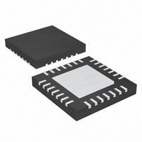
MAX8717ETI+ Maxim Integrated Products, MAX8717ETI+ Datasheet - Page 25

MAX8717ETI+
Manufacturer Part Number
MAX8717ETI+
Description
IC CNTRLR PWR SUP 28-TQFN
Manufacturer
Maxim Integrated Products
Datasheet
1.MAX8717ETI.pdf
(30 pages)
Specifications of MAX8717ETI+
Applications
Controller, Notebook Computers
Voltage - Input
4 ~ 26 V
Number Of Outputs
2
Voltage - Output
3.3V, 5V, 1 ~ 5.5 V
Operating Temperature
0°C ~ 85°C
Mounting Type
Surface Mount
Package / Case
28-TQFN Exposed Pad
Maximum Operating Temperature
+ 85 C
Mounting Style
SMD/SMT
Minimum Operating Temperature
- 40 C
Lead Free Status / RoHS Status
Lead free / RoHS Compliant
shows the input-capacitor RMS current vs. input volt-
age for an application that requires 5V/5A and 3.3V/5A.
This shows the improvement of the 40/60 optimal inter-
leaving over 50/50 interleaving and in-phase operation.
For most applications, nontantalum chemistries (ceramic,
aluminum, or OS-CON) are preferred due to their resis-
tance to power-up surge currents typical of systems
with a mechanical switch or connector in series with the
input. Choose a capacitor that has less than 10°C tem-
perature rise at the RMS input current for optimal relia-
bility and lifetime.
Most of the following MOSFET guidelines focus on the
challenge of obtaining high load-current capability
when using high-voltage (> 20V) AC adapters. Low-
current applications usually require less attention.
The high-side MOSFET (N
the resistive losses plus the switching losses at both
V
should be roughly equal to the losses at V
lower losses in between. If the losses at V
significantly higher, consider increasing the size of N
Conversely, if the losses at V
higher, consider reducing the size of N
not vary over a wide range, optimum efficiency is
achieved by selecting a high-side MOSFET (N
has conduction losses equal to the switching losses.
Choose a low-side MOSFET (N
possible on-resistance (R
ate-sized package (i.e., 8-pin SO, DPAK, or D
and is reasonably priced. Ensure that the
MAX8716/MAX8717/MAX8756/MAX8757 DL_ gate dri-
ver can supply sufficient current to support the gate
charge and the current injected into the parasitic drain-
to-gate capacitor caused by the high-side MOSFET
turning on; otherwise, cross-conduction problems may
occur. Switching losses are not an issue for the low-
side MOSFET since it is a zero-voltage switched device
when used in the step-down topology.
Worst-case conduction losses occur at the duty-factor
extremes. For the high-side MOSFET (N
case power dissipation due to resistance occurs at
minimum input voltage:
Generally, use a small high-side MOSFET to reduce
switching losses at high input voltages. However, the
R
pation limits often limits how small the MOSFET can be.
IN(MIN)
DS(ON)
Interleaved High-Efficiency, Dual Power-Supply
PD N RESISTIVE
and V
required to stay within package power-dissi-
(
H
IN(MAX)
______________________________________________________________________________________
Power MOSFET Selection
. Ideally, the losses at V
)
=
Power MOSFET Dissipation
DS(ON)
H
V
) must be able to dissipate
Controllers for Notebook Computers
V
OUT
IN
IN(MAX)
L
), comes in a moder-
(
) that has the lowest
I
LOAD
are significantly
)
2
H
H
R
. If V
IN(MAX)
), the worst-
DS ON
IN(MIN)
(
IN
IN(MIN)
H
2
)
PAK),
) that
, with
does
are
H
.
The optimum occurs when the switching losses equal
the conduction (R
losses do not become an issue until the input is greater
than approximately 15V.
Calculating the power dissipation in high-side
MOSFETs (N
it must allow for difficult-to-quantify factors that influ-
ence the turn-on and turn-off times. These factors
include the internal gate resistance, gate charge,
threshold voltage, source inductance, and PCB layout
characteristics. The following switching-loss calculation
provides only a very rough estimate and is no substi-
tute for breadboard evaluation, preferably including
verification using a thermocouple mounted on N
where C
Q
N
source/sink current (1A typ).
Switching losses in the high-side MOSFET can become
a heat problem when maximum AC adapter voltages
are applied, due to the squared term in the switching-
loss equation (C x V
chosen for adequate R
becomes extraordinarily hot when subjected to
V
lower parasitic capacitance.
For the low-side MOSFET (N
dissipation always occurs at maximum battery voltage:
The absolute worst case for MOSFET power dissipation
occurs under heavy-overload conditions that are
greater than I
exceed the current limit and cause the fault latch to trip.
To protect against this possibility, “overdesign” the cir-
cuit to tolerate:
where I
limit circuit, including threshold tolerance and sense-
resistance variation. The MOSFETs must have a
relatively large heatsink to handle the overload power
dissipation.
PD N RESISTIVE
IN(MAX)
G(SW) 2
H
MOSFET, and I
(
L
LIMIT
OSS
PD (N SWITCHING)
⎛
⎜
⎝
, consider choosing another MOSFET with
, is the change needed to turn on the
V
IN(MAX) LOAD SW
I
H
is the peak current allowed by the current-
LOAD
is the N
H
) due to switching losses is difficult, since
η
LOAD(MAX)
TOTAL
I
DS(ON)
=
)
IN
=
I
LIMIT
H
f
2
⎡
⎢
⎢
⎣
GATE
, MOSFET's output capacitance,
1
x f
DS(ON)
−
) losses. High-side switching
⎞
⎟
⎠
⎛
⎜
⎝
SW
⎛
⎜
⎝
but are not high enough to
−
=
V
Q
IN MAX
⎛
⎜
⎝
I
V
GATE
G(SW)
). If the high-side MOSFET
is the peak gate-drive
Δ
L
OUT
(
), the worst-case power
I
INDUCTOR
at low battery voltages
⎞
⎟ +
⎠
)
2
⎞
⎟
⎠
⎤
⎥
⎥
⎦
C
(
I
LOAD
OSS IN
⎞
⎟
⎠
V
2
)
2
2
f
R
SW
H
DS ON
:
(
25
)


