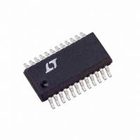
LTC1736IG Linear Technology, LTC1736IG Datasheet - Page 21

LTC1736IG
Manufacturer Part Number
LTC1736IG
Description
IC REG SW SYNC STEPDWN HE 24SSOP
Manufacturer
Linear Technology
Datasheet
1.LTC1736CG.pdf
(28 pages)
Specifications of LTC1736IG
Applications
Converter, Intel Pentium® II, III
Voltage - Input
3.5 ~ 36 V
Number Of Outputs
1
Voltage - Output
0.93 ~ 2 V
Operating Temperature
-40°C ~ 85°C
Mounting Type
Surface Mount
Package / Case
24-SSOP
Lead Free Status / RoHS Status
Contains lead / RoHS non-compliant
Available stocks
Company
Part Number
Manufacturer
Quantity
Price
Part Number:
LTC1736IG
Manufacturer:
LINEAR/凌特
Quantity:
20 000
APPLICATIO S I FOR ATIO
4. Transition losses apply only to the topside MOSFET(s),
Other “hidden” losses such as copper trace and internal
battery resistances can account for an additional 5% to
10% efficiency degradation in portable systems. It is very
important to include these “system” level losses in the
design of a system. The internal battery and fuse resis-
tance losses can be minimized by making sure that C
adequate charge storage and very low ESR at the switch-
ing frequency. A 25W supply will typically require a
minimum of 20 F to 40 F of capacitance having a maxi-
mum of 0.01 to 0.02 of ESR. Other losses including
Schottky conduction losses during dead-time and induc-
tor core losses generally account for less than 2% total
additional loss.
Checking Transient Response
The regulator loop response can be checked by looking at
the load current transient response. Switching regulators
take several cycles to respond to a step in DC (resistive)
load current. When a load step occurs, V
amount equal to I
series resistance of C
discharge C
forces the regulator to adapt to the current change and
return V
time V
ringing, which would indicate a stability problem. OPTI-
LOOP compensation allows the transient response to be
optimized over a wide range of output capacitance and
ESR values. The availability of the I
optimization of control loop behavior but also provides a
0.06 . This results in losses ranging from 3% to 17%
as the output current increases from 1A to 5A for a 1.8V
output, or 4% to 20% for a 1.5V output. Efficiency
varies as the inverse square of V
external components and power level. I
the efficiency to drop at high output currents.
and only become significant when operating at high
input voltages (typically 12V or greater). Transition
losses can be estimated from:
Transition Loss = (1.7)(V
OUT
OUT
can be monitored for excessive overshoot or
OUT
to its steady-state value. During this recovery
generating the feedback error signal that
LOAD
U
OUT
(ESR), where ESR is the effective
. I
U
LOAD
IN
2
also begins to charge or
)(I
TH
W
O(MAX)
pin not only allows
OUT
OUT
2
R losses cause
)(C
for the same
shifts by an
RSS
U
)(f)
IN
has
DC coupled and AC filtered closed-loop response test
point. The DC step, rise time and settling at this test point
truly reflects the closed-loop response. Assuming a pre-
dominantly second order system, phase margin and/or
damping factor can be estimated using the percentage of
overshoot seen at this pin. The bandwidth can also be
estimated by examining the rise time at the pin. The I
external components shown in the Figure 1 circuit will
provide an adequate starting point for most applications.
The I
loop compensation. The values can be modified slightly
(from 0.5 to 2 times their suggested values) to optimize
transient response once the final PC layout is done and the
particular output capacitor type and value have been
determined. The output capacitors need to be selected
because the various types and values determine the loop
feedback factor gain and phase. An output current pulse of
20% to 100% of full-load current having a rise time of 1 s
to 10 s will produce output voltage and I
that will give a sense of the overall loop stability without
breaking the feedback loop. The initial output voltage step
may not be within the bandwidth of the feedback loop, so
the standard second-order overshoot/DC ratio cannot be
used determine phase margin. The gain of the loop will be
increased by increasing R
will be increased by decreasing C
same factor that C
be kept the same, thereby keeping the phase the same in
the most critical frequency range of the feedback loop. The
output voltage settling behavior is related to the stability of
the closed-loop system and will demonstrate the actual
overall supply performance. For a detailed explanation of
optimizing the compensation components, including a
review of control loop theory, refer to Application Note 76.
Improve Transient Response and Reduce Output
Capacitance with Active Voltage Positioning
Fast load transient response, limited board space and low
cost are requirements of microprocessor power supplies.
Active voltage positioning improves transient response
and reduces the output capacitance required to power a
microprocessor where a typical load step can be from 0.2A
TH
series R
C
-C
C
is decreased, the zero frequency will
C
filter sets the dominant pole-zero
C
and the bandwidth of the loop
C
. If R
C
is increased by the
TH
LTC1736
pin waveforms
21
TH


