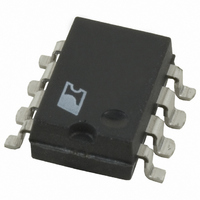
DPA423GN Power Integrations, DPA423GN Datasheet - Page 16

DPA423GN
Manufacturer Part Number
DPA423GN
Description
IC CONV DC-DC DPA SWITCH 8SMD
Manufacturer
Power Integrations
Series
DPA-Switch®r
Specifications of DPA423GN
Applications
Converter, Power Over Ethernet and Telecom Applications
Voltage - Input
16 ~ 75 V
Number Of Outputs
1
Voltage - Output
220V
Operating Temperature
-40°C ~ 125°C
Mounting Type
Surface Mount
Package / Case
8-SMD Gull Wing
Output Voltage
9 V
Output Current
1.75 A
Input Voltage
- 0.3 V to + 220 V
Switching Frequency
282 KHz to 425 KHz
Operating Temperature Range
- 40 C to + 150 C
Mounting Style
SMD/SMT
Duty Cycle (max)
79 %
For Use With
596-1195 - KIT REF DES DPA 6.6W DC-DC CONV596-1009 - KIT DESIGN ACCELERATOR DC-DC596-1007 - KIT DESIGN ACCELERATOR POE CONV
Lead Free Status / RoHS Status
Lead free / RoHS Compliant
Available stocks
Company
Part Number
Manufacturer
Quantity
Price
Company:
Part Number:
DPA423GN
Manufacturer:
PowerInt
Quantity:
200
Company:
Part Number:
DPA423GN
Manufacturer:
POWER
Quantity:
5 000
Part Number:
DPA423GN
Manufacturer:
POWER
Quantity:
20 000
Company:
Part Number:
DPA423GN-TL
Manufacturer:
POWER
Quantity:
14 500
Company:
Part Number:
DPA423GN-TL
Manufacturer:
Power Integrations
Quantity:
88 094
Part Number:
DPA423GN-TL
Manufacturer:
POWER
Quantity:
20 000
reset voltage on the secondary winding directly drives a positive
voltage on the gate of catch MOSFET, Q1. MOSFET Q1
provides a low loss conduction path for a substantial portion
of the primary off-time. An isolated auxiliary winding on L2,
rectified and filtered by D1 and C4, provides the bias supply
for the optocoupler transistor. Output regulation is achieved
by using secondary side voltage reference, U3. The resistor
divider formed by R10 and R11, together with the reference
voltage, determines the output voltage. Diode D3 and C13 form
a soft-finish network that, together with the internal duty cycle
and current limit soft-start of the DPA-Switch, prevent output
overshoot at start-up. Resistor R7 ensures that the soft-finish
capacitor is discharged quickly when the output falls out of
regulation. Control loop response is shaped by R6, C16, R12,
C14, R9, R4 and C5, providing a wide bandwidth and good
phase margin at gain crossover. Since the PWM control in
DPA-Switch is voltage mode, no slope compensation is required
for duty cycles above 50%.
Cost Effective 6.6 W Flyback Converter
The DPA-Switch flyback power supply provides a cost effective
solution for high density PoE and VoIP DC-DC applications.
Figure 26 shows a typical implementation of a single output
flyback converter using the DPA423G. For applications that
require input to output isolation, this simple, low component
count design delivers 6.6 W at 3.3 V from a 36 VDC to 57 VDC
input with a nominal efficiency at 48 VDC of 80%.
Resistor R2 programs the input under-voltage and overvoltage
thresholds to 33 V and 86 V respectively. Resistors R1 and R3
program the internal device current limit. The addition of line
Figure 26. A Cost Effective 6.6 W, 3.3 V Flyback DC-DC Converter.
16
DPA423-426
36 - 57 VDC
J1-1
J1-2
+V
100 V
-V
P
7/05
1 µF
C1
IN
IN
47 pF
200 V
1 MΩ
1%
R1
C2
SMAJ
150A
VR1
619 kΩ
D
S
1%
R2
CONTROL
X
L
1
3
2
8.66 kΩ
F
DPA-Switch
1%
R3
T1
C
DPA423G
U1
9, 10
6, 7
4
5
0.1 µF
50 V
C3
100 Ω
R5
SL43
D2
5.1 Ω
22 µF
10 V
R4
C4
BAV19, SOD323
330 µF
6 V
C5
sense resistor R1 reduces the current limit with increasing input
voltage, preventing excessive overload output current. In this
design the overload output current varies less than ±2.5% across
the entire input voltage range. Controlling the current limit also
reduces secondary component stress and leakage inductance
spikes, allowing the use of a lower V
40 V) Schottky output diode, D2.
The primary side Zener clamp VR1 ensures the peak drain
voltage is kept below the 220 V BV
input surge and overvoltage events. During normal operation,
VR1 does not conduct and C2 is sufficient to limit the peak
drain voltage.
The primary bias winding provides CONTROL pin current after
start-up. Diode D3 rectifies the bias winding, while components
R5 and C8 reduce high frequency switching noise and prevent
peak charging of the bias voltage. Capacitor C3 provides
local decoupling of U1 and should be physically close to the
CONTROL and SOURCE pins. Energy storage for start-up
and auto-restart timing is provided by C4.
The secondary is rectified by D2 and the Low ESR tantalum
output capacitors, C5-C7, minimizing switching ripple and
maximizing efficiency. A small footprint secondary output choke
L1 and ceramic output capacitor C9 are adequate to reduce high
frequency noise and ripple to below 35 mV peak-peak under
full load conditions.
The output voltage is sensed by the voltage divider formed
by resistors R8 and R9 and is fed to the low voltage 1.24 V
reference U3. Feedback compensation is provided by R6, R7
D3
1 µF
50 V
C8
0.33 µF
C10
330 µF
6 V
C6
PC357
U2
CAT431L,
51 Ω
SOT23
R6
U3
1 µH, 2A
L1
330 µF
6 V
C7
1 kΩ
0.1 µF
R7
C11
34 kΩ
20 kΩ
DSS
1%
1%
R8
R9
RRM
rating of U1 under
PI-3806-061704
(30 V rather than
1 µF
10 V
C9
3.3 V, 2 A
J2-1
RTN
J2-2


