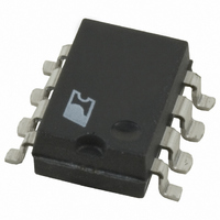
DPA423GN Power Integrations, DPA423GN Datasheet - Page 18

DPA423GN
Manufacturer Part Number
DPA423GN
Description
IC CONV DC-DC DPA SWITCH 8SMD
Manufacturer
Power Integrations
Series
DPA-Switch®r
Specifications of DPA423GN
Applications
Converter, Power Over Ethernet and Telecom Applications
Voltage - Input
16 ~ 75 V
Number Of Outputs
1
Voltage - Output
220V
Operating Temperature
-40°C ~ 125°C
Mounting Type
Surface Mount
Package / Case
8-SMD Gull Wing
Output Voltage
9 V
Output Current
1.75 A
Input Voltage
- 0.3 V to + 220 V
Switching Frequency
282 KHz to 425 KHz
Operating Temperature Range
- 40 C to + 150 C
Mounting Style
SMD/SMT
Duty Cycle (max)
79 %
For Use With
596-1195 - KIT REF DES DPA 6.6W DC-DC CONV596-1009 - KIT DESIGN ACCELERATOR DC-DC596-1007 - KIT DESIGN ACCELERATOR POE CONV
Lead Free Status / RoHS Status
Lead free / RoHS Compliant
Available stocks
Company
Part Number
Manufacturer
Quantity
Price
Company:
Part Number:
DPA423GN
Manufacturer:
PowerInt
Quantity:
200
Company:
Part Number:
DPA423GN
Manufacturer:
POWER
Quantity:
5 000
Part Number:
DPA423GN
Manufacturer:
POWER
Quantity:
20 000
Company:
Part Number:
DPA423GN-TL
Manufacturer:
POWER
Quantity:
14 500
Company:
Part Number:
DPA423GN-TL
Manufacturer:
Power Integrations
Quantity:
88 094
Part Number:
DPA423GN-TL
Manufacturer:
POWER
Quantity:
20 000
Key Application Considerations
DPA-Switch Design Considerations
Power Table
This section provides a description of the assumptions used
to generate the power tables (Tables 1 and 3 through 6) and
explains how to use the information provided by them.
All Power tables: Tables 1 and 3 through 6
• Maximum output power is limited by the device internal
• Data assumes adequate heat sinking to keep the junction
• The use of P and G packages are recommended for device
Forward power tables: Tables 1 (upper half), 3 and 4
• Output power figures are based on forward topology using
• Dissipation data assumes a diode loss representing 6%
Flyback power tables: Tables 1 (lower half), 5 and 6
• Output power and dissipation figures are based on a 5 V
• Device dissipations above 1.5 W are possible using the
The power tables provide two types of information. The first is
the expected device dissipation for a given output power. The
second is the maximum power output. Each table specifies
the input voltage range and assumes a single 5 V output using
Schottky diode rectification.
For example, referring to Table 1, for 36 VDC to 75 VDC input
range, DPA424 would typically dissipate 1 W in a 23 W forward
converter and has a maximum power capacity of 35 W. In the
18
DPA423-426
current limit. This is the peak output power which could
become the continuous output power, provided adequate
heat sinking is used.
temperature at or below 100 °C and worst case R
T
dissipation equal to or less than 1.5 W only due to package
thermal limitation. For device dissipation above 1.5 W, use
S and R packages.
Schottky diode rectification. Up to 5% higher output power
is possible using synchronous rectification.
of the total output power and combined loss in magnetic
components representing 6% of the total output power.
DPA-Switch losses are based on a ratio between conduction
and switching losses of approximately 3:1. These
assumptions are typical for a single 5 V output forward
converter design using Schottky rectification and adequately
designed magnetic components.
output using Schottky diode rectification with an efficiency
of 85%. Values are generated by calculation based on
I
correlated to bench measurement of each DPA-Switch
device.
S and R packages. However the forward converter topology
is recommended for such higher power designs.
2 •
J
= 100 °C.
R
P
7/05
DS(ON)
losses and characterization of switching losses,
DS(ON)
at
Table 5. Flyback Output Power Table for 16-32 VDC Input
Table 3. Output Power Table for 16-32 VDC Input Voltage.
Notes: 1. Limited by device internal current limit. 2. See text in this
section for a complete description of assumptions. 3. See Part Ordering
Information.
Table 4. Output Power Table for 24-48 VDC Input Voltage
Total Device
Table 6. Flyback Output Power Table for 24-48 VDC Input Voltage.
Notes: 1. Maximum output power is limited by device internal
current limit. 2. See text in this section for a complete description of
assumptions. 3. See Part Ordering Information. 4. Higher switching losses
may prevent DPA425 from delivering more power than a smaller device.
Dissipation
Total Device
PRODUCT
Total Device
Dissipation
PRODUCT
Dissipation
PRODUCT
Total Device
PRODUCT
DPA423
DPA424
DPA425
DPA426
Dissipation
DPA423
DPA424
DPA425
DPA426
DPA423
DPA424
DPA425
DPA423
DPA424
Voltage (See Table 3 for Notes).
(See Table 3 for Notes).
16-32 VDC RANGE (FORWARD)
24-48 VDC RANGE (FORWARD)
3
16-32 VDC RANGE (FLYBACK)
3
3
24-48 VDC RANGE (FLYBACK)
OUTPUT POWER TABLE
OUTPUT POWER TABLE
OUTPUT POWER TABLE
3,4
OUTPUT POWER TABLE
0.5 W
10 W 14 W 22 W 27 W
12 W 16.5 W 25 W 31 W 37 W
5 W
7 W
0.5 W 1 W
16 W 22 W 35 W 43 W
18 W 25 W 39 W 48 W 58 W 65 W
11 W 16 W 23.5 W
6.5 W 8.5 W 10 W
8 W 11 W
0.5 W 0.75 W
8.5 W 11.5 W 14 W
5 W
7 W
0.5 W 0.75 W
7 W
10 W 15 W
7 W
1 W
10 W 12 W 15 W
-
-
2.5 W 4 W
2.5 W
-
-
1 W
1 W
-
-
4 W
1.5 W
-
-
1.5 W
-
-
-
-
-
-
6 W
6 W
-
-
-
-
2
2
2
2
Output
Power
Output
11 W
22 W
Power
8.5 W
6 W
17 W
Max
Output
Max
15.5 W
Output
11.5 W
Power
7.5 W
31 W
43 W
Power
25 W
47 W
Max
Max
1
1
1
1


