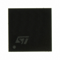
PM6680 STMicroelectronics, PM6680 Datasheet - Page 43

PM6680
Manufacturer Part Number
PM6680
Description
IC CTRLR DUAL STEP DOWN 32VFQFPN
Manufacturer
STMicroelectronics
Datasheet
1.PM6680TR.pdf
(49 pages)
Specifications of PM6680
Applications
Controller, Notebook Power System
Voltage - Input
6 ~ 28 V
Number Of Outputs
2
Voltage - Output
0.9 ~ 5.5 V
Operating Temperature
0°C ~ 85°C
Mounting Type
Surface Mount
Package / Case
32-VFQFN, 32-VFQFPN
Output Voltage
5 V, 0.9 V to 5.5 V, 0.9 V to 3.3 V
Output Current
0.33 A
Input Voltage
5.5 V to 28 V
Mounting Style
SMD/SMT
Maximum Operating Temperature
+ 125 C
Minimum Operating Temperature
- 10 C
For Use With
497-6379 - BOARD EVALUATION FOR PM6680A497-6378 - BOARD EVALUATION FOR PM6680497-6425 - BOARD EVAL BASED ON PM6680A
Lead Free Status / RoHS Status
Lead free / RoHS Compliant
Available stocks
Company
Part Number
Manufacturer
Quantity
Price
Company:
Part Number:
PM6680
Manufacturer:
STMicroelectronics
Quantity:
135
Company:
Part Number:
PM6680
Manufacturer:
INFIONEON
Quantity:
1
Company:
Part Number:
PM6680ATR
Manufacturer:
STMicroelectronics
Quantity:
10 000
Company:
Part Number:
PM6680TR
Manufacturer:
st
Quantity:
1 050
PM6680
Equation 39
OUT2:
Equation 40
Equation 41
(Let's assume Tmax = 75 °C in R
5.
6.
7.
8.
9.
●
●
(Let's assume the maximum temperature Tmax = 75 °C in RDSon calculation)
Input capacitor
Maximum input capacitor RMS current is about 2.8 A. Then I
We put three 10 uF ceramic capacitors with Irms = 1.5 A.
Synchronous rectifier
OUT1: Shottky diode STPS1L30M
OUT2: Shottky diode STPS1L30M
Integrator loop
(Refer to
OUT1: The ripple is smaller than 40mV, then the virtual ESR network is required.
C
C = 5.6 nF; R= 36 kΩ; R1 = 3 kΩ
OUT2: The ripple is smaller than 40 mV, then the virtual ESR network is required.
C
C = 5.6 nF; R = 22 kΩ; R1 = 3.3 kΩ
Output feedback divider
(Refer to
OUT1: R1 = 10 kΩ; R2 = 6.8 kΩ
OUT2: R1 = 11 kΩ; R2 = 1.8 kΩ
Layout guidelines
The layout is very important in terms of efficiency, stability and noise of the system. It is
possible to refer to the PM6680 demoboard for a complete layout example.
For good PC board layout follows these guidelines:
Place on the top side all the power components (inductors, input and output capacitors,
MOSFETs and diodes). Refer them to a power ground plan, PGND. If possible, reserve
a layer to PGND plan. The PGND plan is the same for both the switching sections.
AC current paths layout is very critical (see
minimize their length. Trace the LS MOSFET connection to PGND plan as short as
INT
INT
= 1 nF; C
= 1 nF; C
Figure 37
Figure 30 on page 24
filt
filt
= 110pF; R
= 47 pF; R
)
I
Lvalley
R
R
CSENSE
CSENSE
(min)
INT
INT
DSon
)
=
=1 kΩ
≡
≡
= 1 kΩ
I
100
LOAD
100
calculation)
. 4
4
12
2 .
µ
µ
A
(max)
A
A
A
⋅
⋅
16
16
Figure 41 on page 44
.
.
−
25
25
∆
m
m
I
L
Ω
Ω
(min)
2
≈
≈
670
680
=
Ω
Ω
4
2 .
CinRMS
A
). The first priority is to
Device description
> 2.8 A.
43/49


