L6756D STMicroelectronics, L6756D Datasheet - Page 26

L6756D
Manufacturer Part Number
L6756D
Description
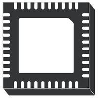
IC CTLR 2/3/4PH BUCK 40-VFQFPN
Manufacturer
STMicroelectronics
Datasheet
1.L6756DTR.pdf
(36 pages)
Specifications of L6756D
Applications
Controller, Intel VR10, VR11, VR11.1
Voltage - Input
12V
Number Of Outputs
4
Voltage - Output
0.3 ~ 1.6 V
Operating Temperature
0°C ~ 70°C
Mounting Type
Surface Mount
Package / Case
40-VFQFN, 40-VFQFPN
Output Voltage
3 V
Input Voltage
- 0.3 V to + 15 V
Switching Frequency
185 KHz to 215 KHz
Operating Temperature Range
- 40 C to + 150 C
Mounting Style
SMD/SMT
Lead Free Status / RoHS Status
Lead free / RoHS Compliant
Available stocks
Company
Part Number
Manufacturer
Quantity
Price
Output voltage monitoring and protections
6
6.1
6.2
26/36
Output voltage monitoring and protections
L6756D monitors through pin VSEN the regulated voltage in order to manage OV and UV.
The device shows different thresholds when in different operative conditions but the
behavior in response to a protection event is still the same as described below.
Overvoltage
Once VCC crosses the turn-ON threshold and the device is enabled (EN = 1), L6756D
provides an overvoltage protection by sensing the regulated voltage through VSEN: when it
overcomes the programmed VID +200 mV (max) the controller:
Feedback disconnection
This feature acts in order to stop the device from regulating dangerous voltages in case the
remote sense connections are left floating. The protection is available for both the positive
and negative sense.
According to what reported in
Figure 11. FB disconnection protection
–
–
–
–
–
–
Permanently sets Gx to zero keeping DRVON high in order to keep all the low-side
MOSFETs on to protect the load.
Drives the OSC/ FLT pin high.
Power supply or EN pin cycling is required to restart operations.
Positive sense consider to monitor the CORE output voltage through both VSEN
and CSxN. As soon as CSxN is more than 650 mV higher than VSEN, the device
latches with all Gx set to HiZ and DRVON set to zero. FLT pin is driven high. In any
case, the 50 μA pull-down current on the VSEN (offset) forces the device to detect
the fault condition.
Negative sense consider to monitor the internal opamp used to recover the SGND
losses by comparing its output and the internal reference generated by the DAC.
As soon as the difference between the output and the input of this opamp is higher
than 500mV, the device latches with all Gx set to HiZ and DRVON set to zero. FLT
pin is driven high.
To recover from a latch condition, cycle VCC or EN.
Figure
11, the protection works as follow:
L6756D


