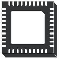
L6756D STMicroelectronics, L6756D Datasheet - Page 30

L6756D
Manufacturer Part Number
L6756D
Description
IC CTLR 2/3/4PH BUCK 40-VFQFPN
Manufacturer
STMicroelectronics
Datasheet
1.L6756DTR.pdf
(36 pages)
Specifications of L6756D
Applications
Controller, Intel VR10, VR11, VR11.1
Voltage - Input
12V
Number Of Outputs
4
Voltage - Output
0.3 ~ 1.6 V
Operating Temperature
0°C ~ 70°C
Mounting Type
Surface Mount
Package / Case
40-VFQFN, 40-VFQFPN
Output Voltage
3 V
Input Voltage
- 0.3 V to + 15 V
Switching Frequency
185 KHz to 215 KHz
Operating Temperature Range
- 40 C to + 150 C
Mounting Style
SMD/SMT
Lead Free Status / RoHS Status
Lead free / RoHS Compliant
Available stocks
Company
Part Number
Manufacturer
Quantity
Price
System control loop compensation
9
30/36
System control loop compensation
The control system can be modeled with an equivalent single-phase converter which only
difference is the equivalent inductor L/N (where each phase has an L inductor and N is the
number of the configured phases). See
Figure 14. Equivalent control loop
The control loop gain results (obtained opening the loop after the COMP pin):
Where:
●
●
●
●
●
●
The Control Loop gain is designed in order to obtain a high DC gain to minimize static error
and to cross the 0 dB axes with a constant -20 dB/dec slope with the desired crossover
frequency ω
poles; both the poles are fixed once the output filter is designed (LC filter resonance ω
and the zero (ω
G
LOOP
R
positioning);
Z
and the applied load R
Z
Z
A(s) is the error amplifier gain;
PWM
P
F
L
LL
s ( )
(s) is the equivalent inductor impedance;
(s) is the compensation network impedance;
(s) is the impedance resulting by the parallel of the output capacitor (and its ESR)
is the equivalent output resistance determined by the droop function (Voltage
=
=
T
–
. Neglecting the effect of Z
----- -
10
-------------------------------------------------------------------------------------------------------------------
[
6
Z
ESR
P
⋅
s ( )
------------------ -
ΔV
V
) is fixed by ESR and the droop resistance.
OSC
+
PWM Z
IN
Z
L
s ( )
is the PWM transfer function.
⋅
]
O
⋅
F
;
s ( )
Z
--------------
A s ( )
F
s ( )
⋅
(
R
+
LL
⎛
⎝
1
+
F
Figure
+
Z
(s), the transfer function has one zero and two
P
----------- -
A s ( )
s ( )
1
)
⎞ R
⎠
14.
⋅
FB
L6756D
LC
)


