ISL6425ERZ Intersil, ISL6425ERZ Datasheet - Page 9
ISL6425ERZ
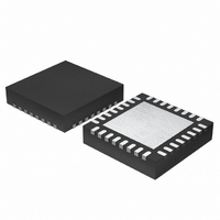
Manufacturer Part Number
ISL6425ERZ
Description
IC REG DUAL LNBP TTL-INP 32-QFN
Manufacturer
Intersil
Datasheet
1.ISL6425ERZ.pdf
(12 pages)
Specifications of ISL6425ERZ
Applications
Converter, Satellite Set-Top Box Designs
Voltage - Input
8 ~ 14 V
Number Of Outputs
2
Voltage - Output
13 ~ 18 V
Operating Temperature
-20°C ~ 85°C
Mounting Type
Surface Mount
Package / Case
32-VQFN Exposed Pad, 32-HVQFN, 32-SQFN, 32-DHVQFN
Lead Free Status / RoHS Status
Lead free / RoHS Compliant
Available stocks
Company
Part Number
Manufacturer
Quantity
Price
Company:

Part Number:
ISL6425ERZ
Manufacturer:
INTERSIL
Quantity:
101


START
SDA
SCL
Byte Format
Every byte put on the SDA line must be 8 bits long. The number
of bytes that can be transmitted per transfer is unrestricted.
Each byte has to be followed by an acknowledge bit. Data is
transferred with the most significant bit first (MSB).
Acknowledge
The master (microprocessor) puts a resistive HIGH level on
the SDA line during the acknowledge clock pulse (Figure 3).
The peripheral that acknowledges has to pull down (LOW)
the SDA line during the acknowledge clock pulse, so that the
SDA line is stable LOW during this clock pulse. (Of course,
set-up and hold times must also be taken into account.)
The peripheral which has been addressed has to generate
an acknowledge after the reception of each byte, otherwise
the SDA line remains at the HIGH level during the ninth
clock pulse time. In this case, the master transmitter can
generate the STOP information in order to abort the transfer.
The ISL6425 will not generate the acknowledge if the
POWER OK signal from the UVLO is LOW.
System Register Format
• R, W = Read and Write bit
• R = Read-only bit
All bits reset to 0 at Power-On
SDA
SCL
CONDITION
START
S
FIGURE 3. ACKNOWLEDGE ON THE I
R, W
R, W
FIGURE 2. START AND STOP WAVEFORMS
SR1
SR2
MSB
1
2
R, W
R, W
9
DCL
X
8
2
C BUS
ACKNOWLEDGE
TABLE 3. SYSTEM REGISTER 1 (SR1)
TABLE 4. SYSTEM REGISTER 2 (SR2)
FROM SLAVE
CONDITION
R, W
R, W
X
X
STOP
P
9
ISL6425
ENT1
R, W
R, W
X
Transmission Without Acknowledge
Avoiding detection of the acknowledgement, the
microprocessor can use a simpler transmission; it waits one
clock without checking the slave acknowledging, and sends
the new data.
This approach, though, is less protected from error and
decreases the noise immunity.
ISL6425 Software Description
Interface Protocol
The interface protocol is comprised of the following, as
shown below in Table 2:
• A start condition (S)
• A chip address byte (MSB on left; the LSB bit determines
• A sequence of data (1 byte + Acknowledge)
• A stop condition (P)
Transmitted Data (
When the R/W bit in the chip is set to 0, the main
microprocessor can write on the system register (SR1) of the
ISL6425 via I
microprocessor as shown below.
S
read (1) or write (0) transmission) (the assigned I
address for the ISL6425 is 0001 00XX)
0
0
LLC1
R, W
R, W
X
0
2
TABLE 2. INTERFACE PROTOCOL
C bus. These will be written by the
1
0
0
I
VSEL1
2
R, W
R, W
EN2
C
0
bus WRITE mode)
R/W ACK Data (8 bits) ACK P
R, W
EN1
OTF
R
February 8, 2005
OLF1
2
C slave
R
R
X
FN9176.1
Related parts for ISL6425ERZ
Image
Part Number
Description
Manufacturer
Datasheet
Request
R

Part Number:
Description:
Single Output LNB Supply and Control Voltage Regulator with I2C Interface for Advanced Satellite Set-top Box Designs
Manufacturer:
INTERSIL [Intersil Corporation]
Datasheet:


Part Number:
Description:
Intersil Corporation [CMOS Serial Controller Interface]
Manufacturer:
Intersil Corporation
Datasheet:
Part Number:
Description:
Manufacturer:
Intersil Corporation
Datasheet:
Part Number:
Description:
357-036-542-201 CARDEDGE 36POS DL .156 BLK LOPRO
Manufacturer:
Intersil Corporation
Datasheet:
Part Number:
Description:
1024-Word x 4-Bit LSI Static RAM
Manufacturer:
Intersil Corporation
Datasheet:
Part Number:
Description:
General Purpose NPN Transistor Arrays FN341.4
Manufacturer:
Intersil Corporation
Datasheet:
Part Number:
Description:
CMOS 16-Bit Microprocessor
Manufacturer:
Intersil Corporation
Datasheet:
Part Number:
Description:
Manufacturer:
Intersil Corporation
Datasheet:
Part Number:
Description:
Manufacturer:
Intersil Corporation
Datasheet:
Part Number:
Description:
Manufacturer:
Intersil Corporation
Datasheet:
Part Number:
Description:
Manufacturer:
Intersil Corporation
Datasheet:
Part Number:
Description:
CMOS 6-Bit Latch and Decoder Memory Interfaces
Manufacturer:
Intersil Corporation
Datasheet:
Part Number:
Description:
CA3046General Purpose NPN Transistor Arrays
Manufacturer:
Intersil Corporation
Datasheet:
Part Number:
Description:
Manufacturer:
Intersil Corporation
Datasheet: