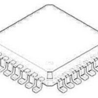
NCP5318FTR2G ON Semiconductor, NCP5318FTR2G Datasheet - Page 26

NCP5318FTR2G
Manufacturer Part Number
NCP5318FTR2G
Description
IC CTLR CPU 2/3/4 PHASE 32-LQFP
Manufacturer
ON Semiconductor
Datasheet
1.NCP5318FTR2G.pdf
(32 pages)
Specifications of NCP5318FTR2G
Applications
Controller, CPU
Voltage - Input
9.5 ~ 13.2 V
Number Of Outputs
4
Operating Temperature
0°C ~ 70°C
Mounting Type
Surface Mount
Package / Case
32-LQFP
Switching Frequency
1 MHz
Mounting Style
SMD/SMT
Primary Input Voltage
18V
No. Of Pins
32
Operating Temperature Range
0°C To +70°C
Termination Type
SMD
Supply Voltage Min
12V
Packaging Type
Tape And Reel
Peak Reflow Compatible (260 C)
Yes
Frequency
1MHz
Rohs Compliant
Yes
Lead Free Status / RoHS Status
Lead free / RoHS Compliant
Voltage - Output
-
Lead Free Status / Rohs Status
Lead free / RoHS Compliant
Other names
NCP5318FTR2G
NCP5318FTR2GOSTR
NCP5318FTR2GOSTR
Available stocks
Company
Part Number
Manufacturer
Quantity
Price
Company:
Part Number:
NCP5318FTR2G
Manufacturer:
ON Semiconductor
Quantity:
10 000
should be performed to insure the design will dissipate the
required power under worst case operating conditions.
Variables considered during testing should include
maximum ambient temperature, minimum airflow,
maximum input voltage, maximum loading and component
variations (i.e., worst case MOSFET R
inductors and capacitors share the MOSFET’s heatsinks and
will add heat and raise the temperature of the circuit board
and MOSFET. For any new design, it is advisable to have as
much heatsink area as possible. All too often, new designs are
found to be too hot and require re−design to add heatsinking.
7. Error Amplifier Tuning
affects transient response and control loop stability. This
loop gain can be adjusted by changing the Error Amplifier’s
high frequency gain, which is done by increasing or
decreasing the Error Amplifier output loading capacitor
(C
characteristic (amplifier output current is proportional to
amplifier input voltage), causing amplifier output voltage to
be proportional to amplifier output load impedance.
be too low, and the converter output voltage may exhibit an
underdamped response to a load transient. On the other
hand, if C
at high frequencies, which may decrease converter output
voltage stability. For initial prototype startup, C
is recommended. When reducing C
ripple voltage at the COMP pin should remain less than
20 mVp−p. Excessive ripple at the COMP pin will
contribute to PWM pulse jitter. In general, the lowest loop
gain that achieves acceptable transient response should be
used.
loop damping in response to load transients as shown in
Figures 26 and 27, where 1430 W was added in series with
the 1.8 nF C
As with any power design, proper laboratory testing
The high frequency gain of the voltage feedback loop
If C
Adding a resistor in series with C
AMP
AMP
). The Error Amplifier has a transconductance
AMP
is too large, the loop gain at high frequencies will
AMP
is too small, there will be too much loop gain
(Adaptive Voltage Positioning not used).
AMP
AMP
will increase control
DS(on)
, peak−to−peak
AMP
). Also, the
= 10 nF
http://onsemi.com
26
Figure 26. Converter Output and COMP Response to
Figure 27. Converter Output and COMP Response to
a Load Step (No Droop), Resistance in Series with
a Load Step (No Droop). 0 W in Series with C
LOAD CURRENT, 60 A/DIV
LOAD CURRENT, 60 A/DIV
OUTPUT VOLTAGE, 50 mV/DIV
COMP VOLTAGE, 100 mV/DIV
OUTPUT VOLTAGE, 50 mV/DIV
COMP VOLTAGE, 100 mV/DIV
20 mS/DIV
20 mS/DIV
Current
C
AMP
AMP


