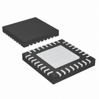
MAX1518BETJ+T Maxim Integrated Products, MAX1518BETJ+T Datasheet - Page 10

MAX1518BETJ+T
Manufacturer Part Number
MAX1518BETJ+T
Description
IC DC-DC CONV TFT-LCD 32-TQFN
Manufacturer
Maxim Integrated Products
Datasheet
1.MAX1518BETJT.pdf
(25 pages)
Specifications of MAX1518BETJ+T
Applications
Converter, TFT, LCD
Voltage - Input
2.6 ~ 6.5 V
Number Of Outputs
1
Voltage - Output
2.6 ~ 13 V
Operating Temperature
-40°C ~ 100°C
Mounting Type
Surface Mount
Package / Case
32-TQFN Exposed Pad
Lead Free Status / RoHS Status
Lead free / RoHS Compliant
TFT-LCD DC-DC Converter with
Operational Amplifiers
10
PIN
17
18
19
20
21
22
23
24
25
26
27
28
29
30
31
32
______________________________________________________________________________________
NAME
COMP
DRVN
OUT4
POS5
NEG5
OUT5
DRVP
COM
DRN
FBN
DEL
FBP
CTL
LX
FB
IN
Operational-Amplifier 4 Output
Operational-Amplifier 5 Noninverting Input
Operational-Amplifier 5 Inverting Input
Operational-Amplifier 5 Output
n-Channel Power MOSFET Drain and Switching Node. Connect the inductor and Schottky diode to LX
and minimize the trace area for lowest EMI.
Supply Voltage Input. IN can range from 2.6V to 6.5V.
Step-Up Regulator Feedback Input. Regulates to 1.236V (nominal). Connect a resistive voltage-divider
from the output (V
Step-Up Regulator Error-Amplifier Compensation Point. Connect a series RC from COMP to AGND.
See the Loop Compensation section for component selection guidelines.
Gate-On Linear-Regulator Feedback Input. FBP regulates to 1.25V (nominal). Connect FBP to the
center of a resistive voltage-divider between the regulator output and AGND to set the gate-on linear-
regulator output voltage. Place the resistive voltage-divider close to the pin.
Gate-On Linear-Regulator Base Drive. Open drain of an internal n-channel MOSFET. Connect DRVP to
the base of an external pnp pass transistor. See the Pass-Transistor Selection section.
Gate-Off Linear-Regulator Feedback Input. FBN regulates to 250mV (nominal). Connect FBN to the
center of a resistive voltage-divider between the regulator output and REF to set the gate-off linear-
regulator output voltage. Place the resistive voltage-divider close to the pin.
Gate-Off Linear-Regulator Base Drive. Open drain of an internal p-channel MOSFET. Connect DRVN to
the base of an external npn pass transistor. See the Pass-Transistor Selection section.
High-Voltage Switch Delay Input. Connect a capacitor from DEL to AGND to set the high-voltage
switch startup delay.
High-Voltage Switch Control Input. When CTL is high, the high-voltage switch between COM and SRC
is on and the high-voltage switch between COM and DRN is off. When CTL is low, the high-voltage
switch between COM and SRC is off and the high-voltage switch between COM and DRN is on. CTL is
inhibited by the undervoltage lockout and when the voltage on DEL is less than 1.25V.
Switch Input. Drain of the internal high-voltage back-to-back p-channel MOSFETs connected to COM.
Internal High-Voltage MOSFET Switch Common Terminal. Do not allow the voltage on COM to exceed
V
SRC
.
MAIN
) to FB to analog ground (AGND). Place the divider within 5mm of FB.
FUNCTION
Pin Description (continued)


