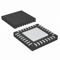
MAX1518BETJ+T Maxim Integrated Products, MAX1518BETJ+T Datasheet - Page 9

MAX1518BETJ+T
Manufacturer Part Number
MAX1518BETJ+T
Description
IC DC-DC CONV TFT-LCD 32-TQFN
Manufacturer
Maxim Integrated Products
Datasheet
1.MAX1518BETJT.pdf
(25 pages)
Specifications of MAX1518BETJ+T
Applications
Converter, TFT, LCD
Voltage - Input
2.6 ~ 6.5 V
Number Of Outputs
1
Voltage - Output
2.6 ~ 13 V
Operating Temperature
-40°C ~ 100°C
Mounting Type
Surface Mount
Package / Case
32-TQFN Exposed Pad
Lead Free Status / RoHS Status
Lead free / RoHS Compliant
(Circuit of Figure 1. V
unless otherwise noted.)
A: OUTPUT VOLTAGE, 1V/div, AC-COUPLED
B: OUTPUT CURRENT, 50mA/div
PIN
10
11
12
13
14
15
16
1
2
3
4
5
6
7
8
9
LOAD-TRANSIENT RESPONSE
OPERATIONAL-AMPLIFIER
400ns/div
NAME
AGND
PGND
BGND
OUT1
NEG1
POS1
OUT2
NEG2
POS2
POS3
OUT3
POS4
NEG4
SRC
SUP
REF
IN
_______________________________________________________________________________________
= 5V, V
MAX1518B toc15
Switch Input. Source of the internal high-voltage p-channel MOSFET. Bypass SRC to PGND with a
minimum 0.1µF capacitor close to the pins.
Reference Bypass Terminal. Bypass REF to AGND with a minimum of 0.22µF close to the pins.
Analog Ground for Step-Up Regulator and Linear Regulators. Connect to power ground (PGND)
underneath the IC.
Power Ground. PGND is the source of the main step-up n-channel power MOSFET. Connect PGND to
the output-capacitor ground terminals through a short, wide PC board trace. Connect to analog ground
(AGND) underneath the IC.
Operational-Amplifier 1 Output
Operational-Amplifier 1 Inverting Input
Operational-Amplifier 1 Noninverting Input
Operational-Amplifier 2 Output
Operational-Amplifier 2 Inverting Input
Operational-Amplifier 2 Noninverting Input
Analog Ground for Operational Amplifiers. Connect to power ground (PGND) underneath the IC.
Operational-Amplifier 3 Noninverting Input
Operational-Amplifier 3 Output
Operational-Amplifier Power Input. Positive supply rail for the operational amplifiers. Typically
connected to V
Operational-Amplifier 4 Noninverting Input
Operational-Amplifier 4 Inverting Input
MAIN
= 13V, V
0V
+50mA
-50mA
0
A
B
MAIN
GON
TFT-LCD DC-DC Converter with
Typical Operating Characteristics (continued)
. Bypass SUP to BGND with a 0.1µF capacitor.
= 24V, V
A: INPUT SIGNAL, 2V/div
B: OUTPUT SIGNAL, 2V/div
LARGE-SIGNAL STEP RESPONSE
GOFF
OPERATIONAL-AMPLIFIER
= -8V, V
1µs/div
Operational Amplifiers
OUT1
FUNCTION
= V
V
MAX1518B toc16
SUP
OUT2
= 6V
= V
0V
0V
A
B
OUT3
A: INPUT SIGNAL, 100mV/div
B: OUTPUT SIGNAL, 100mV/div
= V
SMALL-SIGNAL STEP RESPONSE
OUT4
OPERATIONAL-AMPLIFIER
= V
Pin Description
OUT5
400ns/div
= 6.5V, T
MAX1518B toc17
A
= +25°C
0V
0V
A
B
9


