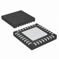
MAX1518BETJ+T Maxim Integrated Products, MAX1518BETJ+T Datasheet - Page 22

MAX1518BETJ+T
Manufacturer Part Number
MAX1518BETJ+T
Description
IC DC-DC CONV TFT-LCD 32-TQFN
Manufacturer
Maxim Integrated Products
Datasheet
1.MAX1518BETJT.pdf
(25 pages)
Specifications of MAX1518BETJ+T
Applications
Converter, TFT, LCD
Voltage - Input
2.6 ~ 6.5 V
Number Of Outputs
1
Voltage - Output
2.6 ~ 13 V
Operating Temperature
-40°C ~ 100°C
Mounting Type
Surface Mount
Package / Case
32-TQFN Exposed Pad
Lead Free Status / RoHS Status
Lead free / RoHS Compliant
The transconductance amplifier regulates the output
voltage by controlling the pass transistor’s base cur-
rent. The total DC loop gain is approximately:
where V
current through the base-to-emitter resistor (R
the MAX1518B, the bias currents for both the gate-on
and gate-off linear-regulator controllers are 0.1mA.
Therefore, the base-to-emitter resistor for both linear
regulators should be chosen to set 0.1mA bias current:
The output capacitor and the load resistance create the
dominant pole in the system. However, the internal
amplifier delay, pass transistor’s input capacitance,
and the stray capacitance at the feedback node create
additional poles in the system, and the output capaci-
tor’s ESR generates a zero. For proper operation, use
the following equations to verify the linear regulator is
properly compensated:
TFT-LCD DC-DC Converter with
Operational Amplifiers
22
1) First, determine the dominant pole set by the linear
regulator’s output capacitor and the load resistor:
The unity-gain crossover of the linear regulator is:
2) The pole created by the internal amplifier delay is
approximately 1MHz:
3) Next, calculate the pole set by the transistor’s
input capacitance, the transistor’s input resistance,
and the base-to-emitter pullup resistor:
______________________________________________________________________________________
A
T
V LR
is 26mV at room temperature, and I
f
POLE LR
_
f
f
POLE IN
where C
CROSSOVER
R
BE
≅
_
_
=
f
10
V
POLE_AMP
T
0 1
=
IN
=
V
.
×
2π
BE
mA
2π
=
= A
×
1
2π
×
g
+
C
=
I
C
m
LOAD MAX LR
f
OUT LR
V_LR
T
0 1
IN
I
0 7
BIAS
I
= 1MHz
.
,
LOAD LR
.
×
R
mA
1
_
IN
V
(
(
R
✕
×
BE
=
f
_
≈
h
POLE_LR
×
FE
6 8
)_
h
||
g
V
. Ω
FE
R
m
OUT LR
IN
k
,
)
×
_
V
REF
BIAS
BE
). For
is the
To ensure stability, choose C
the crossover occurs well before the poles and zero
calculated in steps 2 to 5. The poles in steps 3 and 4
generally occur at several megahertz, and using
ceramic capacitors ensures the ESR zero occurs at
several megahertz as well. Placing the crossover below
500kHz is sufficient to avoid the amplifier-delay pole
and generally works well, unless unusual component
choices or extra capacitances move one of the other
poles or the zero below 1MHz.
g
and f
can be found in the transistor’s data sheet. Because
R
can be simplified:
Substituting for C
4) Next, calculate the pole set by the linear regula-
tor’s feedback resistance and the capacitance
between FB_ and AGND (including stray capaci-
tance):
where C
AGND, R
regulator’s feedback divider, and R
lower resistor of the divider.
5) Next, calculate the zero caused by the output
capacitor’s ESR:
where R
C
m
BE
OUT_LR
f
POLE FB
is the transconductance of the pass transistor,
is much greater than R
T
f
is the transition frequency. Both parameters
POLE ESR
_
ESR
FB
.
UPPER
f
POLE IN
=
is the capacitance between FB_ and
_
is the equivalent series resistance of
2π
f
POLE IN
_
IN
is the upper resistor of the linear
×
=
C
=
and R
2π
_
FB
2π
×
×
=
C
×
(
R
IN
h
C
OUT LR
f
FE
UPPER
T
OUT_LR
IN
1
yields:
1
IN
1
×
_
, the above equation
R
IN
||
×
R
large enough so
R
LOWER
ESR
LOWER
)
is the


