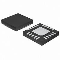
MAX1513ETP+T Maxim Integrated Products, MAX1513ETP+T Datasheet - Page 23

MAX1513ETP+T
Manufacturer Part Number
MAX1513ETP+T
Description
IC CNTRLR TFT-LCD PS 20-TQFN
Manufacturer
Maxim Integrated Products
Datasheet
1.MAX1513ETP.pdf
(28 pages)
Specifications of MAX1513ETP+T
Applications
Controller, TFT, LCD
Voltage - Input
2.7 ~ 5.5 V
Number Of Outputs
1
Voltage - Output
2.7 ~ 50 V
Operating Temperature
-40°C ~ 85°C
Mounting Type
Surface Mount
Package / Case
20-TQFN Exposed Pad
Lead Free Status / RoHS Status
Lead free / RoHS Compliant
determines the frequency placement of the zero and
pole. A typical value of C1 is between 100pF and 10nF.
When adding lead compensation, always check the
loop stability by monitoring the transient response to a
pulsed output load.
Adding lag compensation (the R4/C2 network from FB
to ground in Figure 11) decreases the loop bandwidth
and improves FB noise immunity. Lag compensation
slows the transient response but can increase the stabil-
ity margin, which may be needed for particular compo-
nent choice or high values of FB-divider resistors. Lag
compensation adds a pole-zero pair, attenuating gain at
higher frequencies and lowering loop bandwidth. The
frequencies of the pole and zero for lag compensation
depend on the feedback-divider resistors and the RC
network between FB and GND. The frequencies of the
pole and zero for the lag compensation are:
At high frequencies, R4 is effectively in parallel with R2,
increasing the divider attenuation ratio. If R4 is very
large, the attenuation ratio remains unchanged and as
R4 approaches zero, the attenuation ratio approaches
infinity. A typical value for R4 is greater than 0.1 times
R2. If high-value divider-resistors are used, choose R4
< 1.5kΩ for FB noise immunity. The value of C2 deter-
Figure 11. Feedback Compensation
V
IN
f
f
MAX1513
MAX1514
P LAG
Z LAG
L
_
_
LX
GND
=
=
FB
______________________________________________________________________________________
2
2
π
π
D
×
×
⎛
⎜
⎝
R
R
1
4
4
R1
R2
×
+
C
R
R
TFT-LCD Power-Supply Controllers
1
1
1
2
R3
R4
×
+
C1
C2
R
R
2
2
⎞
⎟ ×
⎠
C
OUT
C
2
R
LOAD
V
MAIN
mines the frequency placement of the pole and zero. A
typical value of C2 is between 100pF and 1000pF.
When adding lag compensation, always check the loop
stability by monitoring the transient response to a
pulsed output load.
The digital soft-start of the main step-up regulator limits
the average input current during startup. If even
smoother startup is needed, add a low-frequency lead-
compensation network (Figure 12). The improved soft-
start is active only during soft-start when the output
voltage rises. Positive changes in the output are instan-
taneously coupled to the FB pin through D1 and the
feed-forward capacitor C1. This arrangement gener-
ates a smoothly rising output voltage. When the output
voltage reaches regulation, capacitor C1 charges up
through R3 and diode D1 turns off. If desired, C1 and
R3 can be chosen to also provide some lead compen-
sation in normal operation. In most applications, lead
compensation in normal operation is not needed and
can be avoided by making R3 large. With R3 much
greater than R1, the pole and the zero in the compen-
sation network are very close to one another after start-
up and cancel out, eliminating the effect of the lead
compensation. With R2 at 10kΩ, an effective value for
C1 is approximately 1000pF.
Figure 12. Using Lead Compensation for Improved Soft-Start
V
IN
MAX1513
MAX1514
L
Using Lead Compensation to Reduce
LX
GND
FB
D
R1
R2
Startup Inrush Current
R3
C1
Charge Pumps
D1
C
OUT
V
MAIN
23


