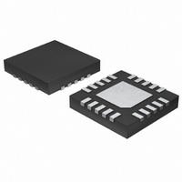
MAX1513ETP+T Maxim Integrated Products, MAX1513ETP+T Datasheet - Page 8

MAX1513ETP+T
Manufacturer Part Number
MAX1513ETP+T
Description
IC CNTRLR TFT-LCD PS 20-TQFN
Manufacturer
Maxim Integrated Products
Datasheet
1.MAX1513ETP.pdf
(28 pages)
Specifications of MAX1513ETP+T
Applications
Controller, TFT, LCD
Voltage - Input
2.7 ~ 5.5 V
Number Of Outputs
1
Voltage - Output
2.7 ~ 50 V
Operating Temperature
-40°C ~ 85°C
Mounting Type
Surface Mount
Package / Case
20-TQFN Exposed Pad
Lead Free Status / RoHS Status
Lead free / RoHS Compliant
TFT-LCD Power-Supply Controllers
8
(Circuit of Figure 1, V
wise noted.)
PIN
1
2
3
4
5
6
7
_______________________________________________________________________________________
MAX1513 MAX1514
OUTB
SUPB
SDFR
FBPB
BUFFER-AMPLIFIER LARGE-SIGNAL
FBN
DEL
REF
NAME
STEP RESPONSE
IN
SDFR
N.C.
N.C.
N.C.
REF
FBN
DEL
= 5V, V
1µs/div
MAIN
Internal Reference. Connect a 0.22µF ceramic capacitor from REF to the analog ground plane,
which is connected to GND. External load capability is at least 100µA.
LCD Shutdown and Frequency-Select Input.
SDFR = GND, LCD shutdown, REF, buffer amplifier and the logic regulator (REG L) output stay on
SDFR = IN, 1.5MHz switching frequency
SDRF = REF, 750kHz switching frequency
SDFR = unconnected, 430kHz switching frequency
Buffer-Amplifier Noninverting Input for the MAX1513. Not internally connected for the MAX1514.
Buffer-Amplifier Output for the MAX1513. Not internally connected for the MAX1514.
Buffer-Amplifier Supply Input for the MAX1513. Bypass to GND with a 0.1µF capacitor. Not internally
connected for the MAX1514.
Gate-Off Linear Regulator (REG N) Feedback Input. FBN regulates to 125mV nominal. Connect to
the center tap of a resistive voltage-divider between the REG N output and the reference voltage
(REF) to set the output voltage. Place the resistive-divider close to this pin.
Delay-Control Timing Capacitor. Connect a capacitor from DEL to GND to set the gate-on linear-
regulator startup delay. See the Power-Up Sequence and Delay Control Block section.
MAX1513/14 toc10
= 15V, V
V
5V/div
AC-COUPLED
V
5V/div
AC-COUPLED
OUTB
FBPB
GON
Typical Operating Characteristics (continued)
= 25V, V
GOFF
= -10V, V
LOGIC
FUNCTION
= 3.3V, V
LOAD-TRANSIENT RESPONSE
GAMMA
BUFFER-AMPLIFIER
1µs/div
= 14.7V, T
Pin Description
MAX1513/14 toc11
A
= +25°C, unless other-
I
50mA/div
V
1V/div
AC-COUPLED
0mA
OUTB
OUTB


