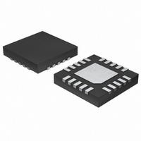
MAX1513ETP+T Maxim Integrated Products, MAX1513ETP+T Datasheet - Page 26

MAX1513ETP+T
Manufacturer Part Number
MAX1513ETP+T
Description
IC CNTRLR TFT-LCD PS 20-TQFN
Manufacturer
Maxim Integrated Products
Datasheet
1.MAX1513ETP.pdf
(28 pages)
Specifications of MAX1513ETP+T
Applications
Controller, TFT, LCD
Voltage - Input
2.7 ~ 5.5 V
Number Of Outputs
1
Voltage - Output
2.7 ~ 50 V
Operating Temperature
-40°C ~ 85°C
Mounting Type
Surface Mount
Package / Case
20-TQFN Exposed Pad
Lead Free Status / RoHS Status
Lead free / RoHS Compliant
where V
current through the base-to-emitter resistor (R
of the four linear-regulator controllers is designed for a
different maximum output current, so they have differ-
ent output drive currents and different bias currents
(I
the Electrical Characteristics table. The current listed in
the conditions column for the FB_ regulation voltage
specification is the individual controller’s bias current.
The base-to-emitter resistor for each controller should
be chosen to set the correct I
The output capacitor and the load resistance create the
dominant pole in the system. However, the internal
amplifier delay, the pass transistor’s input capacitance,
and the stray capacitance at the feedback node create
additional poles in the system. The output capacitor’s
ESR generates a zero. For proper operation, use the
following equations to verify the linear regulator is prop-
erly compensated:
1) First, determine the dominant pole set by the linear
2) The pole created by the internal amplifier delay is
3) Next, calculate the pole set by the transistor’s input
TFT-LCD Power-Supply Controllers
26
BIAS
A
regulator’s output capacitor and the load resistor:
The unity-gain crossover of the linear regulator is:
about 1MHz:
capacitance C
R
______________________________________________________________________________________
V LR
). Each controller’s bias current can be found in
IN
f
POLE LR
_
, and the base-to-emitter pullup resistor:
T
f
POLE IN
f
CROSSOVER
is 26mV at room temperature and I
_
≈
⎛
⎜
⎝
_
V
4
f
T
=
POLE AMP
⎞
⎟ ×
⎠
=
IN
R
2π
, the transistor’s input resistance
BE
_
2π
⎡
⎢
⎢
⎣
=
1
×
+
=
×
C
A
I
LOAD MAX LR
⎛
⎜
⎝
OUT LR
V LR
C
I
I
≈ 1
BIAS
BIAS
BIAS
_
V
IN
I
LOAD LR
BE
_
(
MHz
×
:
1
×
×
(
_
R
f
×
POLE LR
)_
h
BE
FE
V
OUT LR
||
⎞
⎟
⎠
R
_
⎤
⎥
⎥
⎦
IN
×
_
BIAS
)
BE
V
REF
). Each
is the
4) Next, calculate the pole set by the linear regulator’s
5) Next, calculate the zero caused by the output
6) To ensure stability, choose C
f
g
and f
can be found in the transistor’s data sheet. Because
R
can be simplified:
The equation can be further simplified:
feedback resistance and the capacitance between
FB_ and GND (including stray capacitance):
where C
ground, R
regulator’s feedback divider, and R
lower resistor of the divider.
capacitor’s ESR:
where R
of C
so the crossover occurs well before the poles and
zero calculated in steps 2 to 5. The poles in steps 3
and 4 generally occur at several megahertz and
using ceramic capacitors ensures the ESR zero
occurs at several megahertz as well. Placing the
crossover below 500kHz is sufficient to avoid the
amplifier-delay pole and generally works well,
unless unusual component choices or extra capac-
itances move the other poles or zero below 1MHz.
POLE FB
where C
m
BE
is the transconductance of the pass transistor,
f
OUT_LR
POLE ESR
is much greater than R
T
_
is the transition frequency. Both parameters
f
POLE IN
FB
IN
ESR
_
UPPER
=
.
is the capacitance between FB_ and
=
_
is the equivalent series resistance
2π
f
POLE IN
=
2π
g
is the upper resistor of the linear
×
m
=
f
T
2π
C
_
,
2π
FB
R
×
IN
×
=
×
C
=
OUT LR
C
(
h
R
IN
IN
1
f
FE
h
T
UPPER
OUT_LR
1
g
, the above equation
FE
1
m
_
×
,
R
IN
×
||
R
LOWER
large enough
R
LOWER
ESR
is the
)


