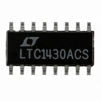
LTC1430ACS Linear Technology, LTC1430ACS Datasheet - Page 13

LTC1430ACS
Manufacturer Part Number
LTC1430ACS
Description
IC SW REG CNTRLR STEP-DWN 16SOIC
Manufacturer
Linear Technology
Type
Step-Down (Buck)r
Datasheet
1.LTC1430ACS8.pdf
(24 pages)
Specifications of LTC1430ACS
Internal Switch(s)
No
Synchronous Rectifier
Yes
Number Of Outputs
1
Voltage - Output
3.3V, Adj
Current - Output
50A
Frequency - Switching
50kHz ~ 500kHz
Voltage - Input
4 ~ 8 V
Operating Temperature
0°C ~ 70°C
Mounting Type
Surface Mount
Package / Case
16-SOIC (3.9mm Width)
Lead Free Status / RoHS Status
Contains lead / RoHS non-compliant
Power - Output
-
Available stocks
Company
Part Number
Manufacturer
Quantity
Price
Company:
Part Number:
LTC1430ACS8
Manufacturer:
LT
Quantity:
10 000
Part Number:
LTC1430ACS8
Manufacturer:
LINEAR/凌特
Quantity:
20 000
Company:
Part Number:
LTC1430ACS8#TRPBF
Manufacturer:
LINEAR
Quantity:
12 711
A
by using a larger RC filter from the PV
work well here. The 10 F capacitor must be VERY close to
the part (preferably right underneath the unit) or output
regulation may suffer.
For both versions of the LTC1430A, PV
than PV
enhance the gate of Q1. This higher voltage can be
provided with a separate supply (typically 12V) which
should power up after PV
simple charge pump (Figure 5). The charge pump consists
of a Schottky diode from PV
capacitor from PV
Q2. This circuit provides 2PV
ON and PV
voltage of the Schottky diode. Ringing at the drain of Q2
can cause transients above 2PV
higher than 7V, a 12V zener diode should be included from
PV
circuitry at PV
More complex charge pumps can be constructed with the
16-lead versions of the LTC1430A to provide additional
voltages for use with standard threshold MOSFETs or very
low PV
provide 2PV
nected to PV
dard threshold MOSFETs to be used with 5V at PV
logic level threshold MOSFETs to be used with 3.3V at
PPLICATI
CC1
to PGND to prevent transients from damaging the
CC
CC
voltages. A tripling charge pump (Figure 7) can
by at least one external MOSFET V
CC
CC
CC2
CC2
– V
and 3PV
4.7 F
O
and PV
CC1
F
or the gate of Q1.
U
while Q1 is OFF where V
+
to the switching node at the drain of
S
CC
CC1
CC
I FOR ATIO
U
C1
220pF
, or it can be generated with a
voltages. These can be con-
100
respectively, allowing stan-
CC
SHUTDOWN
0.1 F
CC
– V
CC
+
to PV
R
7.5k
C
NC
C
4700pF
F
0.01 F
C
CC
W
at PV
to PV
1 F
CC1
pin; 22 and 10 F
CC1
V
SS
FREQSET
SHDN
COMP
Figure 10. 3.3V to 2.5V, 10A Application
PV
must be higher
CC1
CC1
CC
GS(ON)
CC2
LTC1430A
and a 0.1 F
SENSE
; if PV
F
while Q1 is
NC
5V
is the ON
SENSE
PV
U
PGND
–
CC
I
GND
CC1
MAX
to fully
I
G1
G2
FB
FB
MBR0530T1
or 5V
+
CC
is
Q1A, Q1B, Q2: INTERNATIONAL RECTIFIER IRF7801
C
C
IN
OUT
: AVX-TPSE227M010R0100
NC
: AVX-TPSE337M006R0100
PV
allowing the entire system to run from a single 3.3V
supply. Tripling charge pumps require the use of Schottky
diodes to minimize forward drop across the diodes at
start-up. The tripling charge pump circuit will tend to
rectify any ringing at the drain of Q2 and can provide well
more than 3PV
ing factor) circuits should include a 12V zener clamp diode
D
3.3V Input Supply Operation
The LTC1430A can be used with input supply voltages
lower than 5V as long as a low power 5V supply is available
to power the LTC1430A itself and to provide gate drive to
the external MOSFETs. A typical 3.3V to 2.5V application
is shown in Figure 10. The circuit can supply up to 10A at
2.5V output, and draws this power from the 3.3V supply.
The 5V supply typically needs to supply about 20mA to
provide gate drive to the external MOSFETs and keep the
LTC1430A control circuits powered. For applications where
there is no 5V supply available, see the LTC1649 data
sheet.
Compensation and Transient Response
The LTC1430A voltage feedback loop is compensated at
the COMP pin; this is the output node of the internal g
error amplifier. The loop can generally be compensated
16k
Z
CC
to prevent overvoltage at PV
1k
. V
CC
0.1 F
can be driven from the same potential as PV
1 F
CC
3.3V
at PV
Q2
2.7 H/15A
Q1A, Q1B
2 IN PARALLEL
CC1
+
; all tripling (or higher multiply-
+
C
220 F
C
330 F
IN
OUT
4
6
CC1
.
976
1%
1k
1%
1430 F10
2.5V
10A
LTC1430A
13
CC2
m
,


