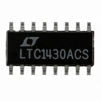
LTC1430ACS Linear Technology, LTC1430ACS Datasheet - Page 5

LTC1430ACS
Manufacturer Part Number
LTC1430ACS
Description
IC SW REG CNTRLR STEP-DWN 16SOIC
Manufacturer
Linear Technology
Type
Step-Down (Buck)r
Datasheet
1.LTC1430ACS8.pdf
(24 pages)
Specifications of LTC1430ACS
Internal Switch(s)
No
Synchronous Rectifier
Yes
Number Of Outputs
1
Voltage - Output
3.3V, Adj
Current - Output
50A
Frequency - Switching
50kHz ~ 500kHz
Voltage - Input
4 ~ 8 V
Operating Temperature
0°C ~ 70°C
Mounting Type
Surface Mount
Package / Case
16-SOIC (3.9mm Width)
Lead Free Status / RoHS Status
Contains lead / RoHS non-compliant
Power - Output
-
Available stocks
Company
Part Number
Manufacturer
Quantity
Price
Company:
Part Number:
LTC1430ACS8
Manufacturer:
LT
Quantity:
10 000
Part Number:
LTC1430ACS8
Manufacturer:
LINEAR/凌特
Quantity:
20 000
Company:
Part Number:
LTC1430ACS8#TRPBF
Manufacturer:
LINEAR
Quantity:
12 711
PI FU CTIO S
G1 (Pin 1/Pin 1): Driver Output 1. Connect this pin to the
gate of the upper N-channel MOSFET, Q1. This output will
swing from PV
is high.
PV
power supply input for G1. G1 will swing from PGND to
PV
PV
an external supply or a simple charge pump connected to
the switching node between the upper MOSFET and the
lower MOSFET; see Applications Information for details.
PGND (Pin 3/Pin 3): Power Ground. Both drivers return to
this pin. It should be connected to a low impedance ground
in close proximity to the source of Q2. 8-lead parts have
PGND and GND tied together at Pin 3.
GND (Pin 4/Pin 3): Signal Ground. All low power internal
circuitry returns to this pin. To minimize regulation errors
due to ground currents, GND should be connected to
PGND right at the LTC1430A. 8-lead parts have PGND and
GND tied together internally at Pin 3.
SENSE
pins connect to the internal resistor divider and to the
internal feedback node. To use the internal divider to set
the output voltage to 3.3V, connect SENSE
terminal of the output capacitor and SENSE
should be left floating in applications that use the internal
divider. To use an external resistor divider to set the output
voltage, float SENSE
nal resistor divider to FB.
SHDN (Pin 8/Pin 5): Shutdown. A TTL compatible low
level at SHDN for longer than 50 s puts the LTC1430A into
shutdown mode. In shutdown, G1 and G2 go low, all
internal circuits are disabled and the quiescent current
drops to 10 A max. A TTL compatible high level at SHDN
allows the part to operate normally.
SS (Pin 9/NA): Soft Start. The SS pin allows an external
capacitor to be connected to implement a soft start func-
tion. An external capacitor from SS to ground controls the
start-up time and also compensates the current limit loop,
allowing the LTC1430A to enter and exit current limit
cleanly. See Applications Information for more details.
CC1
CC1
CC
U
+ V
. PV
(Pin 2/Pin 2): Power V
–
, FB, SENSE
GS(ON)
CC1
U
must be connected to a potential of at least
CC1
(Q1). This potential can be generated using
to PGND. It will always be low when G2
+
U
+
and SENSE
(Pins 5, 6, 7/Pin 4): These three
(16-Lead Package/8-Lead Package)
CC
for Driver 1. This is the
–
and connect the exter-
+
to the positive
–
to GND. FB
COMP (Pin 10/Pin 6): External Compensation. The COMP
pin is connected directly to the output of the error amplifier
and the input of the PWM. An RC network is used at this
node to compensate the feedback loop to provide opti-
mum transient response. See Applications Information for
compensation details.
FREQSET (Pin 11/NA): Frequency Set. This pin is used to
set the free running frequency of the internal oscillator.
With the pin floating, the oscillator runs at about 200kHz.
A resistor from FREQSET to ground will speed up the
oscillator; a resistor to V
tions Information for resistor selection details.
I
old for the internal current limit comparator. If I
below I
limit. I
with an external resistor to PV
source.
I
switched node at the source of Q1 and the drain of Q2
through a 1k resistor. The 1k resistor is required to prevent
voltage transients from damaging I
taken up to 18V above GND without damage.
V
circuits draw their supply from this pin. Connect to a clean
power supply, separate from the main PV
drain of Q1. This pin requires a 4.7 F or greater bypass
capacitor. 8-lead parts have V
at Pin 7 and require at least a 10 F bypass to GND.
PV
power supply input for G2. G2 will swing from GND to
PV
supply. 8-lead parts have V
Pin 7 and require at least a 10 F bypass to GND.
G2 (Pin 16/Pin 8): Driver Output 2. Connect this pin to the
gate of the lower N-channel MOSFET, Q2. This output will
swing from PV
is high.
MAX
FB
CC
CC2
CC2
(Pin 13/NA): Current Limit Sense. Connect to the
(Pin 14/Pin 7): Power Supply. All low power internal
(Pin 12/NA): Current Limit Set. I
MAX
. PV
(Pin 15/Pin 7): Power V
MAX
CC2
has a 12 A pull-down to GND. It can be adjusted
with G1 on, the LTC1430A will go into current
is usually connected to the main high power
CC2
to PGND. It will always be low when G1
CC
will slow it down. See Applica-
CC
CC
and PV
CC
CC
and PV
for Driver 2. This is the
or an external voltage
FB
MAX
CC2
LTC1430A
. This pin can be
CC2
CC
sets the thresh-
tied together at
supply at the
tied together
FB
drops
5


