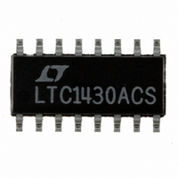
LTC1430ACS Linear Technology, LTC1430ACS Datasheet - Page 3

LTC1430ACS
Manufacturer Part Number
LTC1430ACS
Description
IC SW REG CNTRLR STEP-DWN 16SOIC
Manufacturer
Linear Technology
Type
Step-Down (Buck)r
Datasheet
1.LTC1430ACS8.pdf
(24 pages)
Specifications of LTC1430ACS
Internal Switch(s)
No
Synchronous Rectifier
Yes
Number Of Outputs
1
Voltage - Output
3.3V, Adj
Current - Output
50A
Frequency - Switching
50kHz ~ 500kHz
Voltage - Input
4 ~ 8 V
Operating Temperature
0°C ~ 70°C
Mounting Type
Surface Mount
Package / Case
16-SOIC (3.9mm Width)
Lead Free Status / RoHS Status
Contains lead / RoHS non-compliant
Power - Output
-
Available stocks
Company
Part Number
Manufacturer
Quantity
Price
Company:
Part Number:
LTC1430ACS8
Manufacturer:
LT
Quantity:
10 000
Part Number:
LTC1430ACS8
Manufacturer:
LINEAR/凌特
Quantity:
20 000
Company:
Part Number:
LTC1430ACS8#TRPBF
Manufacturer:
LINEAR
Quantity:
12 711
V
SYMBOL
V
V
I
g
g
A
I
I
t
t
DC
The
temperature range.
Note 1: Absolute Maximum Ratings are those values beyond which the life
of a device may be impaired.
Note 2: All currents into device pins are positive; all currents out of device
pins are negative. All voltages are referenced to ground unless otherwise
specified.
Note 3: Supply current in normal operation is dominated by the current
needed to charge and discharge the external FET gates. This will vary with
ELECTRICAL CHARACTERISTICS
IN
MAX
SS
r
NOV
mV
mI
IH
IL
V
, t
CC
MAX
s
= 5V, T
denotes specifications which apply over the full operating
A
PARAMETER
SHDN Input High Voltage
SHDN Input Low Voltage
SHDN Input Current
Error Amplifier Transconductance
I
Error Amplifier Open-Loop Gain
I
Soft Start Source Current
Driver Rise/Fall Time
Driver Non-Overlap Time
Maximum Duty Cycle
= 25 C (Note 2) unless otherwise noted.
LIM
MAX
Amplifier Transconductance
Sink Current
CONDITIONS
(Note 4)
(Note 5)
V
V
Figure 3, PV
Figure 3, PV
Figure 3, V
V
I(MAX)
SS
FB
= 1.265V
= 0V
= V
COMP
CC
CC1
CC1
= PV
= PV
= V
CC
CC2
CC2
,
= 5V
= 5V
the LTC1430A operating frequency, operating voltage and the external
FETs used.
Note 4: The I
normal (not current limited) operation, the I
Note 5: The open-loop DC gain and transconductance from the FB pin
(SENSE
respectively.
+
and SENSE
LIM
amplifier can sink but cannot source current. Under
–
floating) to COMP pin will be A
MIN TYP MAX
350
2.4
– 8
40
25
90
8
LTC1430AC
2400
93.5
– 12
650 1100
130
48
12
80
0.1
– 16
250
250
0.8
16
1
LIM
MIN
300
2.4
40
–8
25
89
8
output current will be zero.
LTC1430AI
LTC1430A
2400
93.5
TYP MAX
– 12
650 1200
130
V
48
12
80
0.1
and gm
– 17
250
250
0.8
17
1
V
UNITS
3
mho
mho
dB
ns
ns
%
V
V
A
A
A


