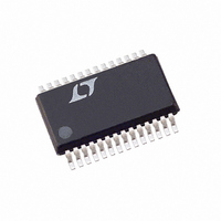
LTC1628CG-SYNC#PBF Linear Technology, LTC1628CG-SYNC#PBF Datasheet - Page 21

LTC1628CG-SYNC#PBF
Manufacturer Part Number
LTC1628CG-SYNC#PBF
Description
IC SW REG STEP-DOWN 28-SSOP
Manufacturer
Linear Technology
Type
Step-Down (Buck)r
Datasheet
1.LTC1628CG-SYNCPBF.pdf
(32 pages)
Specifications of LTC1628CG-SYNC#PBF
Internal Switch(s)
No
Synchronous Rectifier
Yes
Number Of Outputs
2
Voltage - Output
Adj to 0.8V
Current - Output
3A
Frequency - Switching
140kHz ~ 310kHz
Voltage - Input
3.5 ~ 30 V
Operating Temperature
0°C ~ 85°C
Mounting Type
Surface Mount
Package / Case
28-SSOP
Lead Free Status / RoHS Status
Lead free / RoHS Compliant
Power - Output
-
Available stocks
Company
Part Number
Manufacturer
Quantity
Price
APPLICATIO S I FOR ATIO
The phase detector used is an edge sensitive digital type
which provides zero degrees phase shift between the
external and internal oscillators. This type of phase detec-
tor will not lock up on input frequencies close to the
harmonics of the VCO center frequency. The PLL hold-in
range, ∆f
The output of the phase detector is a complementary pair
of current sources charging or discharging the external
filter network on the PLLFLTR pin.
If the external frequency (f
lator frequency f
pulling up the PLLFLTR pin. When the external frequency
is less than f
down the PLLFLTR pin. If the external and internal fre-
quencies are the same but exhibit a phase difference, the
current sources turn on for an amount of time correspond-
ing to the phase difference. Thus the voltage on the
PLLFLTR pin is adjusted until the phase and frequency of
the external and internal oscillators are identical. At this
stable operating point the phase comparator output is
open and the filter capacitor C
LTC1628-SYNC PLLIN pin must be driven from a low
impedance source such as a logic gate located close to the
pin. When using multiple LTC1628-SYNC’s (or LTC1629’s,
as shown in Figure 14) for a phase-locked system, the
PLLFLTR pin of the master oscillator should be biased at
a voltage that will guarantee the slave oscillator(s) ability
to lock onto the master’s frequency. A DC voltage of 0.7V
to 1.7V applied to the master oscillator’s PLLFLTR pin is
recommended in order to meet this requirement. The
resultant operating frequency can range from 170kHz to
270kHz.
The loop filter components (C
current pulses from the phase detector and provide
a stable input to the voltage controlled oscillator. The
filter components C
loop acquires lock. Typically R
to 0.1µF.
∆f
H
= ∆f
H
, is equal to the capture range, ∆f
C
= ±0.5 f
0SC
, current is sunk continuously, pulling
0SC
U
LP
, current is sourced continuously,
O
(150kHz-300kHz)
and R
U
PLLIN
LP
LP
LP
) is greater than the oscil-
LP
=10kΩ and C
determine how fast the
, R
holds the voltage. The
W
LP
) smooth out the
C:
LP
U
is 0.01µF
Minimum On-Time Considerations
Minimum on-time t
that the LTC1628-SYNC is capable of turning on the top
MOSFET. It is determined by internal timing delays and the
gate charge required to turn on the top MOSFET. Low duty
cycle applications may approach this minimum on-time
limit and care should be taken to ensure that
If the duty cycle falls below what can be accommodated by
the minimum on-time, the LTC1628-SYNC will begin to
skip cycles. The output voltage will continue to be regu-
lated, but the ripple voltage and current will increase.
The minimum on-time for the LTC1628-SYNC is generally
less than 200ns. However, as the peak sense voltage
decreases the minimum on-time gradually increases up to
about 300ns. This is of particular concern in forced
continuous applications with low ripple current at light
loads. If the duty cycle drops below the minimum on-time
limit in this situation, a significant amount of cycle skip-
ping can occur with correspondingly larger current and
voltage ripple.
FCB Pin Operation
The FCB pin can be used to regulate a secondary winding
or as a logic level input. Continuous operation is forced on
both controllers when the FCB pin drops below 0.8V.
During continuous mode, current flows continuously in
the transformer primary. The secondary winding(s) draw
current only when the bottom, synchronous switch is on.
When primary load currents are low and/or the V
ratio is low, the synchronous switch may not be on for a
sufficient amount of time to transfer power from the
output capacitor to the secondary load. Forced continuous
operation will support secondary windings providing there
is sufficient synchronous switch duty factor. Thus, the
FCB input pin removes the requirement that power must
be drawn from the inductor primary in order to extract
t
ON MIN
(
)
<
V f
V
IN
OUT
( )
ON(MIN)
LTC1628-SYNC
is the smallest time duration
IN
21
1628syncfa
/V
OUT


