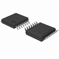
BD9845FV-E2 Rohm Semiconductor, BD9845FV-E2 Datasheet - Page 8

BD9845FV-E2
Manufacturer Part Number
BD9845FV-E2
Description
IC REG SW STEP DOWN 1CH 14-SSOP
Manufacturer
Rohm Semiconductor
Type
Step-Down (Buck)r
Datasheet
1.BD9845FV-E2.pdf
(16 pages)
Specifications of BD9845FV-E2
Internal Switch(s)
No
Synchronous Rectifier
No
Number Of Outputs
1
Current - Output
1A
Frequency - Switching
100kHz ~ 1.5MHz
Voltage - Input
3.6 ~ 35 V
Operating Temperature
-40°C ~ 85°C
Mounting Type
Surface Mount
Package / Case
14-SSOP
Power - Output
500mW
Lead Free Status / RoHS Status
Lead free / RoHS Compliant
Voltage - Output
-
Lead Free Status / Rohs Status
Lead free / RoHS Compliant
Other names
BD9845FV-E2TR
© 2009 ROHM Co., Ltd. All rights reserved.
BD9845FV
www.rohm.com
4) Soft start (soft start function)
5) PWM Comp - DEAD TIME (Pause period adjusting circuit - dead time)
6) OCP Comp (overcurrent detection circuit)
It is possible to provide SS terminal (13pin) with soft start function by
connecting C
Soft start time TSS is shown by the formula below:
Tss = Css・
(Ex) When Css = 0.01 uF
In order to function soft start, time must be set longer enough than
start time of power supply and STB.
It is also possible to provide function of soft start by connecting the
resistor (R1/R2) and capacitor (C
on the right.
Dead time can be set by applying voltage dividing resistance between VREF and GND to DT terminal.
PWM Comp compares the input dead time voltage (DT terminal voltage) and error voltage from Err Amp (FB terminal
voltage) with triangular wave, and turns off and on the output. When dead time voltage < error voltage, duty of output is
determined by dead time voltage. (When dead time setting is not used, pull up DT terminal to VREF terminal with resistor
approx 10 k ohms.)
Dead time voltage VDT in Fig 32 is shown by the formula below:
Be careful when oscillation frequency is high, upper/lower limit of triangular
wave (Vt100/Vt0) is shifted by delay time of comparator to directions
expanding amplitude.
Relation between VDT and Duty [See the graph on the right.]
This function provides protection by forcibly turning off the output when
abnormal overcurrent flows due to shorting of output, etc. When voltage
between terminal OCP+(8pin)/OCP-(9pin) monitoring the current with
sense resistor exceeds overcurrent detection voltage (50 mV typ), it is
determined as overcurrent condition, and switching operation is stopped
immediately by setting OUT to "H" and DT,SS (and FB) to "L".
It is automatically recovered when voltage between terminal OCP+/OCP-
is below overcurrent detection voltage.
In addition, although hysteresis, etc. are not set here, minimum detection
retention time (1.6ms typ) is set for suppressing the heating of FET, etc.
(See the timing chart.)
When the overcurrent detection circuit is not used, short-circuit both
terminal OCP+/OCP- to VCC pin.
When f = 1.5MHz
When f = 100kHz
Tss =
VDT = VREF・
=
SS
5 [msec]
as shown on the right.
0.01×10
Issso
Vinv
2×10
1.95
min
1.9
R1+R2
-6
-6
R2
×1
Css : SS terminal connection capacity
Vinv : Error amplifier reference voltage
(1V typ)
Issso : SS source current (2uA typ)
Duty 100%
DT
typ
2.0
2.1
) to DT terminal (14pin) as shown
max
2.25
2.1
1.35
min
1.4
8/15
Duty 0%
1.5
typ
1.5
[Unit : V]
1.65
max
1.6
Css
of current
Direction
resistor
C
INV
Sense
SS
DT
2.4
2.2
1.8
1.6
1.4
1.2
13
12
2
1
100
VIN
Fig.32
1Vtyp.
OCP+
OCP-
Fig.33
VREF
R 1
R 2
8
9
Fig.35
Fig.34
fosc[KHz]
2009.05 - Rev.A
Technical Note
2uA
50mVtyp.
1000
14
1
VREF
DT
Vt100
OCP Comp
Vt0
ErrAmp
10000


