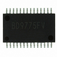
BD9775FV-E2 Rohm Semiconductor, BD9775FV-E2 Datasheet - Page 5

BD9775FV-E2
Manufacturer Part Number
BD9775FV-E2
Description
IC REG SW STEP DOWN HE 28-SSOP
Manufacturer
Rohm Semiconductor
Type
Step-Down (Buck)r
Specifications of BD9775FV-E2
Internal Switch(s)
No
Synchronous Rectifier
Yes
Number Of Outputs
2
Current - Output
400mA
Frequency - Switching
100kHz
Voltage - Input
6 ~ 30 V
Operating Temperature
-40°C ~ 85°C
Mounting Type
Surface Mount
Package / Case
28-SSOP
Power - Output
640mW
Mounting Style
SMD/SMT
Lead Free Status / RoHS Status
Lead free / RoHS Compliant
Voltage - Output
-
Lead Free Status / Rohs Status
Lead free / RoHS Compliant
Other names
BD9775FV-E2TR
●Function Explanation
© 2011 ROHM Co., Ltd. All rights reserved.
BD9775FV
www.rohm.com
1. DC/DC Converter
2. Channel Control
3. Protection
・Reference Voltage
・Internal Regulator A (VREGA)
・Internal regulator B (VREGB)
・Oscillator
・Error Amplifier
・PWM Comparator
・MOSFET Driver
Each output can be individually turned on or off with CTL1 and CTL2. When the CTL is “H” (more than 1.5V), it becomes
turned on.
・Over Current Protection(OCP)
・Short Circuit Protection(SCP)
・Under Voltage Lock Out(UVLO)
・Thermal Shut Down(TSD)
Stable voltage of compensated temperature, is generated from the power supply voltage (VCC). The reference voltage
is 3.0V, the accuracy is ±1%. Place a capacitor with low ESR (several decades mΩ) between VREF and GND.
5V is generated the power supply voltage. The voltage is for the driver of the synchronous rectification’s MOSFET.
Place a capacitor with low ESR (several decades mΩ) between VREGA and PGND.
(VCC-5V) is generated from the power supply voltage. The voltage is for the driver of the main MOSFET switch.
Place a capacitor with low ESR (several decades mΩ) between VREGB and PVCC.
Placing a resistor and a capacitor to RT and CT, respectively, generates two triangle waves for both cannels, and each
wave is opposite phase. The waves are input to the PWM comparators for CH1 and CH2. Also, the oscillating
frequency can be slightly adjusted (less than 20%) by putting external clock pulse into Fin pin, which is higher frequency
than the fixed one.
It amplifies the difference, between the establish output voltage and the actual output one detected at INV. And amplified
voltage comes out from FB.
compensated externally by placing a resistor and a capacitor between INV and FB.
It converts the output voltage from error amplifier into PWM waveform, then output to MOSFET driver.
The main drivers (OUT1, OUT2H) are for P-channel MOSFETs, and the driver (OUT2L) for synchronous rectification is
for N-channel MOSFET. The values of output voltage are clamp to VREGB, VREGA, respectively. All drivers’ output
configurations are push-pull type. In addition, the output current capability is 36mA for the sink current and 320mA
(Vds=0.4V) for the source current.
When detected over current (detecting drop voltage of the main MOSFET’s ON resistance), the MOSFET switch
becomes turned off, and the energy on DTC pin is discharged. After discharged, the output restarts automatically.
The level of the OCP detection threshold can be set by the resistance, which is connected between VCC and CL.
When either output goes down and the voltage on INV pin gets lower than 0.7V, a capacitor placed on SCP is started to
charge.
When the SCP pin becomes more than 2.0V, the main MOSFET switches of both outputs are turned off; then, the
outputs are latched. While they are latched, the IC can be reset by restarting VCC or CTL, or discharging SCP.
Due to avoiding malfunctions when the IC is started up or the power supply voltage is rapidly disconnected, the main
MOSFET switches become off and DTC is discharged when the supply voltage is less than 5.7V. Also, when the
output is latched because of SCP function, the latch becomes reset. Due to preventing malfunctions in the case the
power supply voltage fluctuate at near UVLO threshold, there is 0.1V hysteresis between the detection and reset
voltage of UVLO threshold.
Due to preventing breakdown of the IC by heating up, the main MOSFET switches become off and DTC pin is
discharged by detecting over temperature of the chip. Due to preventing malfunctions in the case temperature fluctuate
at near TSD threshold, there is hysteresis between TSD on and off.
The comparing voltage is 1.0V and the accuracy is ±2%. The phase can be
5/14
Technical Note
2011.05 - Rev.A


