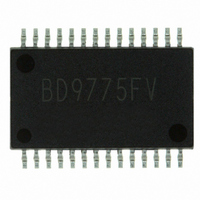
BD9775FV-E2 Rohm Semiconductor, BD9775FV-E2 Datasheet - Page 7

BD9775FV-E2
Manufacturer Part Number
BD9775FV-E2
Description
IC REG SW STEP DOWN HE 28-SSOP
Manufacturer
Rohm Semiconductor
Type
Step-Down (Buck)r
Specifications of BD9775FV-E2
Internal Switch(s)
No
Synchronous Rectifier
Yes
Number Of Outputs
2
Current - Output
400mA
Frequency - Switching
100kHz
Voltage - Input
6 ~ 30 V
Operating Temperature
-40°C ~ 85°C
Mounting Type
Surface Mount
Package / Case
28-SSOP
Power - Output
640mW
Mounting Style
SMD/SMT
Lead Free Status / RoHS Status
Lead free / RoHS Compliant
Voltage - Output
-
Lead Free Status / Rohs Status
Lead free / RoHS Compliant
Other names
BD9775FV-E2TR
© 2011 ROHM Co., Ltd. All rights reserved.
BD9775FV
www.rohm.com
2) Oscillator Synchronization by External Pulse Signal
3) Setting the Over Current Threshold Level
At the operation the oscillator is externally synchronized, input the synchronization signal into Fin in addition to connect a
resistor and a capacitor at RT and CT, respectively. Input the external clock pulse on Fin, which is higher frequency than
the fixed one. However, the frequency variation should be less than 20%. Also, the duty cycle of the pulse should be set
from 10% to 90%.
Short Fin to GND if the function of external synchronization is not needed.
The OCP detection level (Iocp) is determined by the ON resistance (R
(Rcl) which is placed between CL and VCC.
To prevent a malfunction caused by noise, place a capacitor (Ccl) parallel to Rcl.
If OCP function is not needed, short VS to VCC, and short CL to GND.
Iocp =
CT
Fin
With OCP
VS
CL
Rcl
R
ON
Fig.4 CT Waveform during Synchronized with External Pulse
×10
To Main MOSFET Drain
Rcl
Ccl
-5
Fig.5 Without Synchronization Signal
[A] (typ.)
Fig.6 CL, VS Pin Connection
Fin
VCC
7/14
Without OCP
ON
) of the main MOSFET switch and the resistance
VS
CL
: Fixed with RT and CT
: Synchronized
VCC
Technical Note
2011.05 - Rev.A


