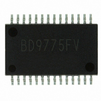
BD9775FV-E2 Rohm Semiconductor, BD9775FV-E2 Datasheet - Page 27

BD9775FV-E2
Manufacturer Part Number
BD9775FV-E2
Description
IC REG SW STEP DOWN HE 28-SSOP
Manufacturer
Rohm Semiconductor
Type
Step-Down (Buck)r
Specifications of BD9775FV-E2
Internal Switch(s)
No
Synchronous Rectifier
Yes
Number Of Outputs
2
Current - Output
400mA
Frequency - Switching
100kHz
Voltage - Input
6 ~ 30 V
Operating Temperature
-40°C ~ 85°C
Mounting Type
Surface Mount
Package / Case
28-SSOP
Power - Output
640mW
Mounting Style
SMD/SMT
Lead Free Status / RoHS Status
Lead free / RoHS Compliant
Voltage - Output
-
Lead Free Status / Rohs Status
Lead free / RoHS Compliant
Other names
BD9775FV-E2TR
9) Applications with modes that reverse VCC and pin potentials may cause
10) Timing resistor and capacitor
11) The Dead time input voltage has to be set more than 1.1V.
12) The energy on DTC1(8pin)and DTC2(9pin)is discharged when CTL1(12pin)and CTL2(13pin)are OFF, respectively, or VCC(14pin)
13) If Gate capacitance of P-channel MOSFET or resistance placed on
14) IC pin input
Also, the resistance between DTC and VREF is used more than 30kΩ to work OCP function reliably.
For example, such damage might occur when VCC is shorted with the
GND pin while an external capacitor is charged.
It is recommended to insert a diode for preventing back current flow
in series with VCC or bypass diodes between VCC and each pin.
Gate is large, and the time from beginning of Gate switching to the end of Drain’s (tsw),
is long, it may not start up due to the OCP malfunction.
To avoid it, select MOSFET or adjust resistance as tsw becomes less than 270nsec.
damage to internal IC circuits.
Timing resistor(capacitor) connected between RT(CT) and GND, has to be placed near RT(CT) terminal 3pin(4pin). And pattern has to be short
enough.
This monolithic IC contains P+ isolation and PCB layers between adjacent elements in order to keep them isolated.
P/N junctions are formed at the intersection of these P layers with the N layers of other elements to create a variety
of parasitic elements. For example, when a resistor and transistor are connected to pins as shown in following chart,
○the P/N junction functions as a parasitic diode when GND > (Pin A) for the resistor or GND > (Pin B) for the transistor (NPN).
○Similarly, when GND > (Pin B) for the transistor (NPN), the parasitic diode described above combines with the N layer of other adjacent
elements to operate as a parasitic NPN transistor.
The formation of parasitic elements as a result of the relationships of the potentials of different pins is an
inevitable result of the IC's architecture. The operation of parasitic elements can cause interference with circuit
operation as well as IC malfunction and damage. For these reasons, it is necessary to use caution so that the IC is
not used in a way that will trigger the operation of parasitic elements, such as by the application of voltages lower
than the GND (PCB) voltage to input and output pins.
(PINA)
is OFF (UVLO activation). However, it is considerable to occur overshoot when CTL and VCC are turned on with remaining more than 1V on
the DTC.
N
P
P
pd(W)
+
1.0
0.8
0.6
0.4
0.2
Resistor
0
N
0
GND
P
② 0.85W
①
Parasitic element
VREF
AMBIENT TEMPERATURE
25
0.64W
P
+
50
VCC
① 0.587W
(PINB)
N
75
Parasitic element or transistor
P
+
C
Transistor(NPN)
100
P substrate
N
B
GND
P
125
Fig.12
:
E
Fig.11
27/29
Ta(℃)
150
P
+
②Copper laminate area 70 mm×70mm
①With no heat sink
N
Countercurrent
prevention diode
Parasitic element or transistor
(PINB)
B
C
E
GND
GATE
DRAIN
Fig.9
Vcc
(PINA)
Parasitic element
Pin
Fig.10
Bypass diode
tsw


