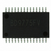
BD9775FV-E2 Rohm Semiconductor, BD9775FV-E2 Datasheet - Page 5

BD9775FV-E2
Manufacturer Part Number
BD9775FV-E2
Description
IC REG SW STEP DOWN HE 28-SSOP
Manufacturer
Rohm Semiconductor
Type
Step-Down (Buck)r
Specifications of BD9775FV-E2
Internal Switch(s)
No
Synchronous Rectifier
Yes
Number Of Outputs
2
Current - Output
400mA
Frequency - Switching
100kHz
Voltage - Input
6 ~ 30 V
Operating Temperature
-40°C ~ 85°C
Mounting Type
Surface Mount
Package / Case
28-SSOP
Power - Output
640mW
Mounting Style
SMD/SMT
Lead Free Status / RoHS Status
Lead free / RoHS Compliant
Voltage - Output
-
Lead Free Status / Rohs Status
Lead free / RoHS Compliant
Other names
BD9775FV-E2TR
●Pin configuration
●Block functional descriptions
・Error amp
・Oscillator (OSC)
・ SLOPE
・PWM COMP
・Reference voltage (5Vreg,33Vreg)
・External synchronization (SYNC)
・Over current protection (OCP)
・Sequence control (Sequence DET)
・Protection circuits (UVLO/TSD)
EXTVCC
COMP2
DGND2
VREG5
OUTL2
BD9011KV(VQFP48C)
Oscillation frequency is determined by the switching frequency pin (RT) in this block. The frequency can be set between 250kHz and 550kHz.
SLOPE block. Switching duty is limited to a percentage of the internal maximum duty, and thus cannot be 100% of the maximum.
Over current protection is activated when the VCCCL-CL voltage reaches or exceeds 90mV. When over current protection is active, Duty is low,
The error amp compares output feedback voltage to the 0.8V reference voltage and provides the comparison result as COMP voltage, which is
The SLOPE block uses the clock produced by the oscillator to generate a triangular wave, and sends the wave to the PWM comparator.
The PWM comparator determines switching Duty by comparing the COMP voltage, output from the error amp, with the triangular wave from the
This block generates the internal reference voltages: 5V and 3.3V.
Determines the switching frequency, based on the external pulse applied.
and output voltage also decreases. When LOFF=L, the output voltage has fallen to 70% or below and output is latched OFF. The OFF latch
mode ends when the latch is set to STB, EN.
Compares FB voltage with reference voltage (0.56V) and outputs the result as DET.
The UVLO lock out function is activated when VREG falls to about 2.8V, while TSD turns outputs OFF when the chip temperature reaches or
exceeds 150℃. Output is restored when temperature falls back below the threshold value.
used to determine the switching Duty. COMP voltage is limited to the SS voltage, since soft start at power up is based on SS pin voltage.
SW2
SS2
FB2
N.C
N.C
N.C
N.C
37
38
39
40
41
42
43
44
45
46
47
48
36
1
35
2
34
3
33
4
32
5
31
Fig-15
6
30
7
29
8
28
9
27
10
26
11
12
25
5/29
24
23
22
21
20
19
18
17
16
15
14
13
DET1
SS1
COMP1
FB1
N.C
VREG33
N.C
VREG5A
N.C
OUTL1
DGND1
SW1
●
No.
Pin
10
11
12
13
14
15
16
17
18
19
20
21
22
23
24
25
26
27
28
29
30
31
32
33
34
35
36
37
38
39
40
41
42
43
44
45
46
47
48
Pin function table
1
2
3
4
5
6
7
8
9
Pin name
VREG5A
EXTVCC
VCCCL2
VCCCL1
VREG33
COMP1
COMP2
OUTH2
BOOT2
BOOT1
OUTH1
DGND1
VREG5
DGND2
OUTL1
OUTL2
GNDS
SYNC
LOFF
DET1
DET2
VCC
SW1
GND
SW2
STB
EN1
EN2
LLM
CL2
CL1
FB1
SS1
SS2
FB2
N.C
N.C
N.C
N.C
N.C
N.C
N.C
N.C
N.C
N.C
N.C
N.C
RT
External synchronous pulse input pin
Over current detection setting pin 1
Over current protection OFF latch
Switching frequency setting pin
High side FET gate drive pin 2
High side FET gate drive pin 1
Low side FET gate drive pin 1
Low side FET gate drive pin 2
Over current detection VCC2
Built-in pull-down resistor pin
Reference input REG output
Over current detection pin 2
Over current detection CC1
High side FET source pin 1
High side FET source pin 2
Low side FET source pin 1
Low side FET source pin 2
Non-connect (unused) pin
Non-connect (unused) pin
Non-connect (unused) pin
Non-connect (unused) pin
Non-connect (unused) pin
Non-connect (unused) pin
Non-connect (unused) pin
Non-connect (unused) pin
Non-connect (unused) pin
Non-connect (unused) pin
Non-connect (unused) pin
Non-connect (unused) pin
OUTH2 driver power pin
OUTH1 driver power pin
External power input pin
FET drive REG output
Soft start setting pin 1
Soft start setting pin 2
Output 1 ON/OFF pin
Output 2 ON/OFF pin
FET drive REG input
Standby ON/OFF pin
FB detector output 1
function ON/OFF pin
FB detector output 2
Error amp output 1
Error amp output 2
Error amp input 1
Error amp input 2
Input power pin
Sense ground
Function
Ground


