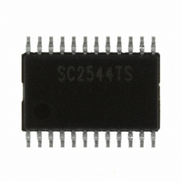
SC2544TSTRT Semtech, SC2544TSTRT Datasheet - Page 17

SC2544TSTRT
Manufacturer Part Number
SC2544TSTRT
Description
IC CTRL/REG SYNC BUCK 24-TSSOP
Manufacturer
Semtech
Type
Step-Down (Buck)r
Datasheet
1.SC2544TSTRT.pdf
(24 pages)
Specifications of SC2544TSTRT
Internal Switch(s)
No
Synchronous Rectifier
No
Number Of Outputs
2
Voltage - Output
Adj to 0.75V
Frequency - Switching
100kHz ~ 300kHz
Voltage - Input
4.5 ~ 28 V
Operating Temperature
-40°C ~ 85°C
Mounting Type
Surface Mount
Package / Case
24-TSSOP
Lead Free Status / RoHS Status
Lead free / RoHS Compliant
Current - Output
-
Power - Output
-
Other names
SC2544TSTR
PC Board Layout Issues
PC Board Layout Issues
P P P P P o o o o o w w w w w er Stage
PC Board Layout Issues
PC Board Layout Issues
PC Board Layout Issues
Circuit board layout is very important for the proper
operation of high frequency switching power con-
verters. A power ground plane is required to reduce
ground bounces. The followings are suggested for
proper layout.
1) Separate the power ground from the signal ground. In
SC2544 design, use an isolated local ground plane for
the controller and tie it to power grand.
2) Minimize the size of the high pulse current loop.
Keep the top MOSFET, the bottom MOSFET and the
input capacitors within a small area with short and
wide traces. In addition to the aluminum energy
storage capacitors, add multi-layer ceramic (MLC)
capacitors from the input to the power ground to
improve high frequency bypass.
3) Reduce high frequency voltage ringing. Widen and
shorten the drain and source traces of the MOSFETs
to reduce stray inductances. Add a small RC snubber
if necessary to reduce the high frequency ringing at
the phase node. Sometimes slowing down the gate
drive signal also helps in reducing the high frequency
ringing at the phase node if the EMI is a concern for
the system.
4) Shorten the gate drive trace. Integrity of the
gate drive (voltage level, leading and falling edges)
is important for circuit operation and efficiency. Short
and wide gate drive traces reduce trace inductances.
Bond wire inductance is about 2~3nH. If the length of
the PCB trace from the gate driver to the MOSFET
gate is 1 inch, the trace inductance will be about
25nH. If the gate drive current is 2A with 10ns rise
and falling times, the voltage drops across the bond
wire and the PCB trace will be
respectively. This may slow down the switching
transient of the MOSFET’s. These inductances may
also ring with the gate capacitance.
supplies (BST and PVCC) close to the IC and power
ground.
POWER MANAGEMENT
Applications Information (Cont.)
5) Put the decoupling capacitor for the gate drive power
2005 Semtech Corp.
er Stage
er Stage
er Stage
er Stage
0.6V and 5V
17
Control Section
Control Section
Control Section
Control Section
Control Section
6) The frequency-setting resistor Rosc should be placed
close to Pin 23. Trace length from this resistor to the
analog ground should be minimized.
7) Place the bias decoupling capacitor right across
the VCC and analog ground AGND.
www.semtech.com
SC2544


