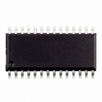
L6712ADTR STMicroelectronics, L6712ADTR Datasheet - Page 12

L6712ADTR
Manufacturer Part Number
L6712ADTR
Description
IC CTRLR DC/DC 2PH SYNC 28SOIC
Manufacturer
STMicroelectronics
Type
Step-Down (Buck)r
Datasheet
1.L6712AQTR.pdf
(29 pages)
Specifications of L6712ADTR
Internal Switch(s)
No
Synchronous Rectifier
Yes
Number Of Outputs
2
Voltage - Output
0.9 ~ 3.3 V
Current - Output
2A
Frequency - Switching
150kHz
Voltage - Input
12V
Operating Temperature
0°C ~ 70°C
Mounting Type
Surface Mount
Package / Case
28-SOIC (7.5mm Width)
Power - Output
2W
Operating Temperature Range
- 40 C to + 125 C
Mounting Style
SMD/SMT
Lead Free Status / RoHS Status
Contains lead / RoHS non-compliant
Other names
497-4218-2
L6712A L6712
circuitry reads the current during the time in which the low-side mosfet is on (OFF Time). During this time,
the reaction keeps the pin ISENx and PGNDSx at the same voltage while during the time in which the
reading circuitry is off, an internal clamp keeps these two pins at the same voltage sinking from the ISENx
pin the necessary current (Needed if low-side mosfet R
imum rating overcome on ISENx pin).
The proprietary current reading circuit allows a very precise and high bandwidth reading for both positive
and negative current. This circuit reproduces the current flowing through the sensing element using a high
speed Track & Hold transconductance amplifier. In particular, it reads the current during the second half
of the OFF time reducing noise injection into the device due to the mosfet turn-on (See Figure 8-left). Track
time must be at least 200ns to make proper reading of the delivered current.
This circuit sources a constant 50µA current from the PGNDSx pin: it must be connected through the Rg
resistor to the ground side of the sensing element (See Figure 8-right). The two current reading circuitries
use this pin as a reference keeping the ISENx pin to this voltage.
The current that flows in the ISENx pin is then given by the following equation:
Where R
ductance resistor used between ISENx and PGNDSx pins toward the reading points; I
carried by the relative phase. The current information reproduced internally is represented by the second
term of the previous equation as follow:
Since the current is read in differential mode, also negative current information is kept; this allow the de-
vice to check for dangerous returning current between the two phases assuring the complete equalization
between the phase's currents. From the current information of each phase, information about the total cur-
rent delivered (I
taken. I
current carried by the two phases.
Figure 8. Current reading timing (left) and circuit (right)
The transconductance resistor Rg can be designed in order to have current information of 25µA per phase
at full nominal load; the over current intervention threshold is set at 140% of the nominal (I
According to the above relationship, the over current threshold (I
placed at 1/2 of the total delivered maximum current, results:
12/29
INFOX
SENSE
I
I
I
LS1
LS2
FB
is then compared to I
is an external sense resistor or the R
FB
= I
INFO1
I
ISENx
+I
INFO2
Track & Hold
=
) and the average current for each phase (I
50µA
AVG
I
INFOx
to give the correction to the PWM output in order to equalize the
+
R
------------------------------------------------ -
SENSE
=
R
------------------------------------------------ -
SENSE
R
⋅
g
dsON
I
PHASEx
dsON
R
⋅
g
I
of the low side mosfet and R
PHASEx
sense is implemented to avoid absolute max-
PGNDSx
LGATEx
=
ISENx
50µA
OCPx
) for each phase, which has to be
+
I
INFOx
I
Rg
Rg
ISENx
50
AVG
µ
A
= (I
PHASEx
INFO1
g
is the transcon-
INFOx
+I
is the current
INFO2
= 35µA).
)/2 ) is


