MIC2182-5.0YM Micrel Inc, MIC2182-5.0YM Datasheet - Page 14
MIC2182-5.0YM
Manufacturer Part Number
MIC2182-5.0YM
Description
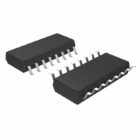
IC CTRLR SYNC BUCK 5.0V 16-SOIC
Manufacturer
Micrel Inc
Type
Step-Down (Buck)r
Datasheet
1.MIC2182-5.0YSM.pdf
(28 pages)
Specifications of MIC2182-5.0YM
Internal Switch(s)
No
Synchronous Rectifier
Yes
Number Of Outputs
1
Voltage - Output
5V
Current - Output
20A
Frequency - Switching
300kHz
Voltage - Input
4.5 ~ 16.5 V
Operating Temperature
-40°C ~ 85°C
Mounting Type
Surface Mount
Package / Case
16-SOIC (3.9mm Width)
Power - Output
400mW
Lead Free Status / RoHS Status
Lead free / RoHS Compliant
Other names
576-2158
MIC2182-5.0YM
MIC2182-5.0YM
Available stocks
Company
Part Number
Manufacturer
Quantity
Price
Company:

Part Number:
MIC2182-5.0YM
Manufacturer:
MICREL
Quantity:
48
Company:
Part Number:
MIC2182-5.0YM
Manufacturer:
MICREL
Quantity:
784
Part Number:
MIC2182-5.0YM
Manufacturer:
MICREL/麦瑞
Quantity:
20 000


MIC2182
The enable pin (pin 6) has two threshold levels, allowing the
MIC2182 to shut down in a low current mode, or turn off output
switching in UVLO mode. An enable pin voltage lower than
the shutdown threshold turns off all the internal circuitry and
reduces the input current to typically 0.1 A.
If the enable pin voltage is between the shutdown and UVLO
thresholds, the internal bias, V
turned on. The soft-start pin is forced low by an internal
discharge MOSFET. The output drivers are inhibited from
switching and remain in a low state. Raising the enable
voltage above the UVLO threshold of 2.5V allows the soft-
start capacitor to charge and enables the output drivers.
Either of two UVLO conditions will pull the soft-start capacitor
low.
MOSFET Gate Drive
The MIC2182 high-side drive circuit is designed to switch an
N-channel MOSFET. Referring to the block diagram in Figure
2, a bootstrap circuit, consisting of D2 and C
energy to the high-side drive circuit. Capacitor C
charged while the low-side MOSFET is on and the voltage on
the V
MOSFET driver is turned on, energy from C
the MOSFET on. As the MOSFET turns on, the voltage on the
V
versed biased and C
the high-side MOSFET on. When the low-side switch is
turned back on, C
The drive voltage is derived from the internal 5V V
supply. The nominal low-side gate drive voltage is 5V and the
nominal high-side gate drive voltage is approximately 4.5V
due the voltage drop across D2. A fixed 80ns delay between
the high- and low-side driver transitions is used to prevent
current from simultaneously flowing unimpeded through both
MOSFETs.
M9999-042204
SW
• When the V
• When the enable pin drops below the 2.5V
SW
pin increases to approximately V
threshold
pin (pin 15) is approximately 0V. When the high-side
Figure 8. Sync Waveforms
BST
DD
BST
drops below 4.1V
is recharged through D2.
floats high while continuing to keep
DD
, and reference voltages are
TIME
IN
. Diode D2 is re-
BST
BST
is used to turn
, supplies
DD
BST
bias
is
14
Oscillator and Sync
The internal oscillator is free running and requires no external
components. The nominal oscillator frequency is 300kHz. If
the output voltage is below approximately 0.95V, the oscilla-
tor operates in a frequency-foldback mode and the switching
frequency is reduced to 60kHz.
The SYNC input (pin 5) allows the MIC2182 to synchronize
with an external clock signal. The rising edge of the sync
signal generates a reset signal in the oscillator, which turns
off the low-side gate drive output. The high-side drive then
turns on, restarting the switching cycle. The sync signal is
inhibited when the controller operates in skip mode or during
frequency foldback. The sync signal frequency must be
greater than the maximum specified free running frequency
of the MIC2182. If the synchronizing frequency is lower,
double pulsing of the gate drive outputs will occur. When not
used, the sync pin must be connected to ground.
Figure 8 shows the timing between the external sync signal
(trace 2), the low-side drive (trace 1) and the high-side drive
(trace R1). There is a delay of approximately 250ns between
the rising edge of the external sync signal and turnoff of the
low-side MOSFET gate drive.
Some concerns of operating at higher frequencies are:
• Higher power dissipation in the internal V
regulator. This occurs because the MOSFET
gates require charge to turn on the device. The
average current required by the MOSFET gate
increases with switching frequency. This in-
creases the power dissipated by the internal
V
charge which can be driven by the MIC2182
over the input voltage range, for different values
of switching frequency. The total gate charge
includes both the high- and low-side MOSFETs.
The larger SOP package is capable of dissipat-
ing more power than the SSOP package and
can drive larger MOSFETs with higher gate
drive requirements.
DD
regulator. Figure 10 shows the total gate
Figure 9. Startup Waveforms
TIME
April 22, 2004
DD
Micrel
Related parts for MIC2182-5.0YM
Image
Part Number
Description
Manufacturer
Datasheet
Request
R

Part Number:
Description:
IC CTRLR SYNC BUCK 5.0V 16-SSOP
Manufacturer:
Micrel Inc
Datasheet:
Part Number:
Description:
IC CTRLR SYNC BUCK 3.3V 16-SSOP
Manufacturer:
Micrel Inc
Datasheet:

Part Number:
Description:
IC CTRLR SYNC BUCK 3.3V 16-SOIC
Manufacturer:
Micrel Inc
Datasheet:
Part Number:
Description:
IC CTRLR SYNC BUCK 3.3V 16-SOIC
Manufacturer:
Micrel Inc
Datasheet:
Part Number:
Description:
IC CTRLR SYNC BUCK 3.3V 16-SSOP
Manufacturer:
Micrel Inc
Datasheet:
Part Number:
Description:
IC CTRLR SYNC BUCK 5.0V 16-SSOP
Manufacturer:
Micrel Inc
Datasheet:
Part Number:
Description:
IC CTRLR SYNC BUCK 3.3V 16-SOIC
Manufacturer:
Micrel Inc
Datasheet:
Part Number:
Description:
IC CTRLR SYNC BUCK 5.0V 16-SOIC
Manufacturer:
Micrel Inc
Datasheet:
Part Number:
Description:
IC CTRLR SYNC BUCK 3.3V 16-SSOP
Manufacturer:
Micrel Inc
Datasheet:
Part Number:
Description:
IC CTRLR SYNC BUCK 5.0V 16-SSOP
Manufacturer:
Micrel Inc
Datasheet:

Part Number:
Description:
Manufacturer:
Micrel Inc
Datasheet:
Part Number:
Description:
Manufacturer:
Micrel Inc
Datasheet:
Part Number:
Description:
Manufacturer:
Micrel Inc
Datasheet:
Part Number:
Description:
Manufacturer:
Micrel Inc
Datasheet:
Part Number:
Description:
Manufacturer:
Micrel Inc
Datasheet: