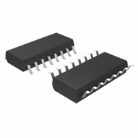
MIC2182-5.0YM Micrel Inc, MIC2182-5.0YM Datasheet - Page 17

MIC2182-5.0YM
Manufacturer Part Number
MIC2182-5.0YM
Description
IC CTRLR SYNC BUCK 5.0V 16-SOIC
Manufacturer
Micrel Inc
Type
Step-Down (Buck)r
Datasheet
1.MIC2182-5.0YSM.pdf
(28 pages)
Specifications of MIC2182-5.0YM
Internal Switch(s)
No
Synchronous Rectifier
Yes
Number Of Outputs
1
Voltage - Output
5V
Current - Output
20A
Frequency - Switching
300kHz
Voltage - Input
4.5 ~ 16.5 V
Operating Temperature
-40°C ~ 85°C
Mounting Type
Surface Mount
Package / Case
16-SOIC (3.9mm Width)
Power - Output
400mW
Lead Free Status / RoHS Status
Lead free / RoHS Compliant
Other names
576-2158
MIC2182-5.0YM
MIC2182-5.0YM
Available stocks
Company
Part Number
Manufacturer
Quantity
Price
Company:
Part Number:
MIC2182-5.0YM
Manufacturer:
MICREL
Quantity:
48
Company:
Part Number:
MIC2182-5.0YM
Manufacturer:
MICREL
Quantity:
784
Part Number:
MIC2182-5.0YM
Manufacturer:
MICREL/麦瑞
Quantity:
20 000
charge can be a significant source of power dissipation in the
MIC2182. At low output load this power dissipation is notice-
able as a reduction in efficiency. The average current re-
quired to drive the high-side MOSFET is:
where:
The low-side MOSFET is turned on and off at V
because the freewheeling diode is conducting during this
time. The switching losses for the low-side MOSFET is
usually negligable. Also, the gate drive current for the low-
side MOSFET is more accurately calculated using C
V
For the low-side MOSFET:
Since the current from the gate drive comes from the input
voltage, the power dissipated in the MIC2182 due to gate
drive is:
A convenient figure of merit for switching MOSFETs is the on-
resistance times the total gate charge (R
numbers translate into higher efficiency. Low gate-charge
logic-level MOSFETs are a good choice for use with the
MIC2182. Power dissipation in the MIC2182 package limits
the maximum gate drive current. Refer to Figure 10 for the
MIC2182 gate drive limits.
Parameters that are important to MOSFET switch selection
are:
The voltage rating of the MOSFETs are essentially equal to
the input voltage. A safety factor of 20% should be added to
the V
due to circuit parasitics.
The power dissipated in the switching transistor is the sum of
the conduction losses during the on-time (P
switching losses that occur during the period of time when the
MOSFETs turn on and off (P
where:
Making the assumption the turn-on and turnoff transition
times are equal, the transition time can be approximated by:
April 22, 2004
MIC2182
DS
• Voltage rating
• On-resistance
• Total gate charge
= 0 instead of gate charge.
DS(max)
I
Q
R
I
I
P
P
P
P
G[high-side](avg)
G[high-side](avg)
G[low-side](avg)
gate drive
SW
conduction
AC
SW
G
average high-side MOSFET gate current
taken from manufacturer’s data sheet
with V
= total gate charge for the high-side MOSFET
= on-resistance of the MOSFET switch.
P
P
of the MOSFETs to account for voltage spikes
AC(off)
conduction
GS
V
= 5V.
I
IN G[high-side](avg)
SW
=
P
I
(rms)
C
AC(on)
Q
ISS
G
P
AC
2
f
AC
S
V
R
GS
).
SW
f
S
I
G[low-side](avg)
DS(on)
conduction
Q
G
) and the
). Lower
DS
ISS
= 0
at
17
where:
The total high-side MOSFET switching loss is:
where:
The low-side MOSFET switching losses are negligible and
can be ignored for these calculations.
RMS Current and MOSFET Power Dissipation Calculation
Under normal operation, the high-side MOSFET’s RMS
current is greatest when V
low-side MOSFET’s RMS current is greatest when V
(minimum duty cycle). However, the maximum stress the
MOSFETs see occurs during short circuit conditions, where
the output current is equal to I
Resistor section). The calculations below are for normal
operation. To calculate the stress under short circuit condi-
tions, substitute I
below to calculate D under short circuit conditions.
The RMS value of the high-side switch current is:
where:
Converter efficiency depends on component parameters,
which have not yet been selected. For design purposes, an
efficiency of 90% can be used for V
can be used for V
more accurately calculated once the design is complete. If the
assumed efficiency is grossly inaccurate, a second iteration
through the design procedure can be made.
For the high-side switch, the maximum dc power dissipation
is:
C
I
t
V
f
D = duty cycle of the converter
P
D
I
I
D
P
t
G
T
S
SW(highside)
SW(low side)
T
AC
D
switch1(dc)
ISS
short circuit
= efficiency of the converter.
= switching transition time
it the switching frequency, nominally 300kHz
= gate drive current (1A for the MIC2182)
(typically 20ns to 50ns)
= freewheeling diode drop, typically 0.5V.
V
C
and C
OUT
(V
ISS
V
IN
IN
overcurrent(max)
(rms)
OSS
(rms)
IN
V
V ) I
R
GS
D
0.063 1.8 10
greater than 10V. The efficiency can be
DS(on)1
are measured at V
I
G
PK
C
IN
OSS
D
1 D I
is low (maximum duty cycle). The
t
overcurrent(max)
I
T
SW1
for I
I
V
OUT(max)
f
IN
S
(rms)
OUT(max)
OUT(max)
IN
3
less than 10V and 85%
2
V
DS
IN
2
2
. Use the formula
. (See the Sense
= 0.
I
PP
12
I
PP
12
M9999-042204
2
2
IN
is high
Micrel


